Near infrared light-control storer and manufacturing method thereof

A technology of near-infrared light and manufacturing methods, which is applied in static memory, digital memory information, semiconductor/solid-state device manufacturing, etc., can solve the problems of small biological penetration depth, tissue damage, etc., achieve convenient and efficient regulation, and realize multi-bit storage , the effect of good application prospects

Inactive Publication Date: 2017-02-22
SHENZHEN UNIV
View PDF3 Cites 7 Cited by
  • Summary
  • Abstract
  • Description
  • Claims
  • Application Information

AI Technical Summary

Problems solved by technology

The biological penetration depth of visible light is small and may damage tissues, which has certain limitations in the application of implantable and wearable flexible electronic devices

Method used


Image

  • Near infrared light-control storer and manufacturing method thereof
  • Near infrared light-control storer and manufacturing method thereof
  • Near infrared light-control storer and manufacturing method thereof

Examples


Embodiment Construction

[0030] In order to make the object, technical solution and advantages of the present invention more clear and definite, the present invention will be further described in detail below with reference to the accompanying drawings and examples. It should be understood that the specific embodiments described here are only used to explain the present invention, not to limit the present invention.

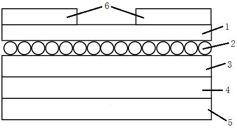
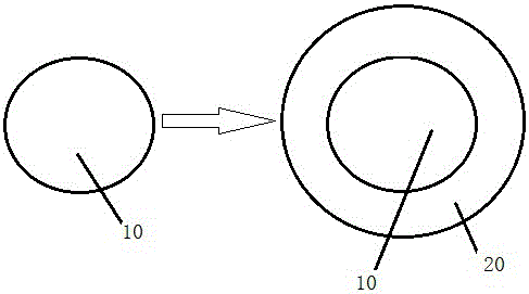
[0031] Conventional memories, which are mostly based on silicon technology, cannot be fabricated on flexible substrates, while storing only single-bit data in a single transistor. Organic electronic devices have the characteristics of light weight, flexibility and low cost. Organic light-controlled memory has become an important development direction in the field of information storage in the future. Compared with visible light, near-infrared light has a greater biological penetration depth and no damage to tissues, and has bright application prospects in implantable and wearable electro...


PUM


Abstract

The invention provides a near infrared light-control storer and a manufacturing method thereof. The near infrared light-control storer comprises a semiconductor layer, a floating gate layer, a dielectric layer, a grid electrode and a substrate, a gold electrode is arranged on the semiconductor layer, and the floating gate layer is formed by coating fluorescent nanoparticles with silicon dioxide. Under control of near infrared light, a storing window is enhanced to realize more-bit storage. Compared with conventional methods of improving material characteristics of the semiconductor layer or enhancing carrier capturing capability of the floating gate layer, utilizing near infrared light for real-time control and for enhancing the storing window has good application prospect in the field of information encryption. Near infrared light control is convenient and efficient and can be combined with the conventional methods to obtain high-performance storers.

Description

technical field [0001] The invention relates to the technical field of memory manufacturing, in particular to a near-infrared light-controlled memory and a manufacturing method thereof. Background technique [0002] Memory is an electronic device with memory function, which has received extensive attention in the field of semiconductor industry, accounting for more than 20% of the entire semiconductor industry. Over the past few decades, the traditional memory has been updated, the size has changed from huge to smaller, and the storage capacity has changed from tiny to larger. At the same time, the storage speed has also been greatly improved. With the rapid development of information technology, people have higher and higher requirements for memory components used to store information, not only must have small device size, ultra-high storage capacity and fast read and write speed, but also have low cost , low power consumption and high reliability characteristics. [000...

Claims


Application Information

Patent Timeline
Patent Type & Authority Applications(China)
IPC IPC(8): H01L51/05H01L51/40G11C13/04
CPCG11C13/04H10K10/474H10K10/466
Inventor 周晔韩素婷
Owner SHENZHEN UNIV
Why Eureka
Try Eureka