Design method for saving space by using high-density connector wafer

A technology that saves space and design method, applied in the field of SI design of server single board, can solve the problems of many holes for reflow and high wiring requirements, and achieve the effect of improving performance, saving PCB space and improving integration.

Inactive Publication Date: 2017-02-22
ZHENGZHOU YUNHAI INFORMATION TECH CO LTD
View PDF4 Cites 3 Cited by
  • Summary
  • Abstract
  • Description
  • Claims
  • Application Information

AI Technical Summary

Problems solved by technology

Adding a driver poses a challenge to the layout of the board
[0004] At the same time, the input and output of the signal driver chip are all high-speed wiring, the wiring requirements are high, and there are many return holes, which also pose challenges to the wiring and wiring space of other signals

Method used


Image

  • Design method for saving space by using high-density connector wafer

Examples


Embodiment 1

[0022] S1. Select driver chips with different driving capabilities in combination with high-speed link channel performance requirements and cost control requirements;

[0023] S2. Put the driver chip on the connector;

[0024] S3. In combination with link conditions, the long link is turned on and the short link is turned off by software.

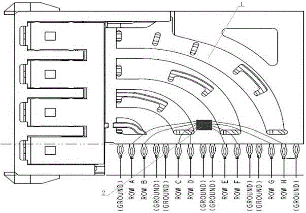
[0025] According to product cost control requirements, you can choose to place driver chips with different driving capabilities on the wafer. Connector customization, combined with link conditions, long links need to be driven, and short links do not need to be driven. Control the opening and closing of the number of driver channels through software to achieve performance control and cost control, increase the layout and wiring space of the single board, and meet the design requirements of si for high-speed link performance.

[0026] The driver chip is a repeater (repeater) with pre-emphasis function to improve link driving capability.

Embodiment 2

[0028] S1. Select driver chips with different driving capabilities in combination with high-speed link channel performance requirements and cost control requirements;

[0029] S2. Put the driver chip on the connector;

[0030] S3. In combination with link conditions, the long link is turned on and the short link is turned off by software.

[0031] According to product cost control requirements, you can choose to place driver chips with different driving capabilities on the wafer. Connector customization, combined with link conditions, long links need to be driven, and short links do not need to be driven. Control the opening and closing of the number of driver channels through software to achieve performance control and cost control, increase the layout and wiring space of the single board, and meet the design requirements of si for high-speed link performance.

[0032] The driver chip is a repeater (repeater) with an equalizing function to improve link driving capability. ...

Embodiment 3

[0034] S1. Select driver chips with different driving capabilities in combination with high-speed link channel performance requirements and cost control requirements;

[0035] S2. Put the driver chip on the connector;

[0036] S3. In combination with link conditions, the long link is turned on and the short link is turned off by software.

[0037] According to product cost control requirements, you can choose to place driver chips with different driving capabilities on the wafer. Connector customization, combined with link conditions, long links need to be driven, and short links do not need to be driven. Control the opening and closing of the number of driver channels through software to achieve performance control and cost control, increase the layout and wiring space of the single board, and meet the design requirements of si for high-speed link performance.

[0038] The driver chip is a driver with an equalization function to improve link driving capability.


PUM


Abstract

The invention discloses a design method for saving space by using a high-density connector wafer. The method comprises: S1, selecting driver chips with different drive capabilities based on combination of performance requirements of a high-speed link channel and a cost control requirement; S2, placing the driver chips on a connector; and S3, opening driving of a long link and closing driving of a short link are realized by using software according to link situations. Compared with the prior art, the method disclosed by the invention has the following beneficial effects: because the drivers are arranged on the connector wafer, the integration of the high-speed connector is improved; the driver chip space on the single board can be saved, so that the space is left for the layout and wiring of the single board; and the method is simple and is easy to use and the operability is high, so that the method is easy to implement in design and manufacturing.

Description

technical field [0001] The invention relates to the field of server single board SI design, in particular to a space-saving design method using a high-density port connector wafer. Background technique [0002] Electrical connectors are used in many electronic systems. It is often easier and more cost-effective to manufacture a system on several printed circuit boards ("PCBs") connected to each other by electrical connectors. A traditional arrangement for connecting several PCBs is to have one PCB as the backplane. Other PCBs called daughter boards or daughter cards are then connected via this backplane by electrical connectors. [0003] In the field of server system signal integrity, with the growth of high-speed signal links, it is often necessary to increase the driver (driver) on a single board to improve the driving capability. A single board usually has many components and a compact layout. Adding a driver poses a challenge to the layout of the board. [0004] At ...

Claims


Application Information

Patent Timeline
Patent Type & Authority Applications(China)
IPC IPC(8): H01R13/66
CPCH01R13/6691H01R2201/04
Inventor 王伟
Owner ZHENGZHOU YUNHAI INFORMATION TECH CO LTD
Why Eureka
Try Eureka