Manufacturing method of electrodes with medium impeding discharging of plasma
A production method and plasma technology, applied in the field of plasma, can solve the problems of poor stability and adaptability, high power supply performance and function requirements, internal discharge, ignition, sound and even combustion, etc., achieve standardization of specifications and tolerances, and low power supply performance requirements , the effect of perfect production process
- Summary
- Abstract
- Description
- Claims
- Application Information
AI Technical Summary
Problems solved by technology
Method used
Image
Examples
Embodiment 1
[0032] Example 1: Design example of small space purification medium hindering discharge electrode
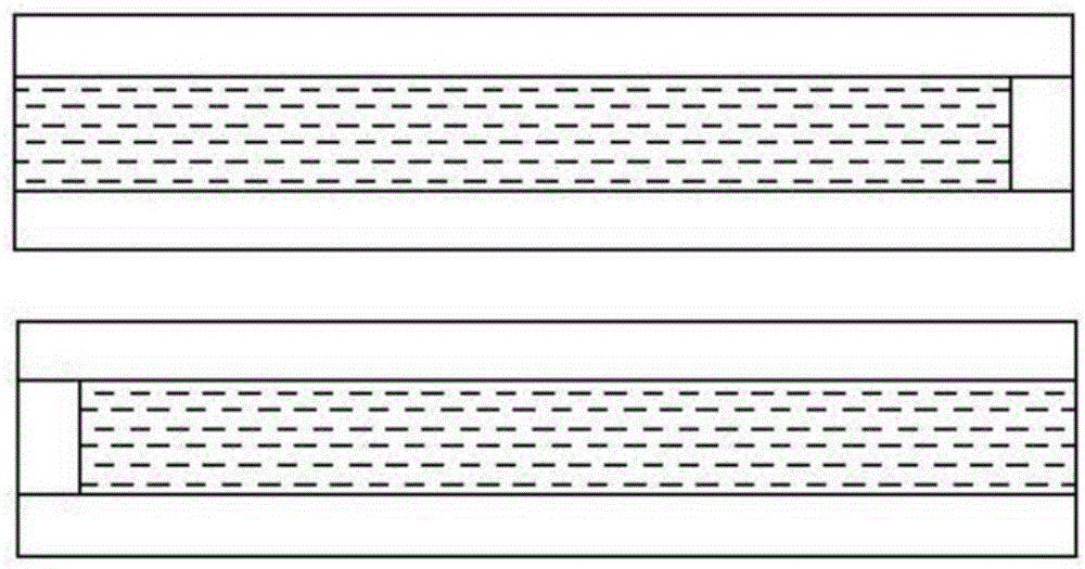
[0033] The hindering medium is selected from one of quartz tubes or ceramic tubes. The dimensions of the quartz tubes or ceramic tubes are as follows: outer diameter 1mm±0.01mm, inner diameter 0.05mm±0.01mm, length 40mm±0.1mm;
[0034] Coating a conductive layer on the inner wall of the quartz tube or ceramic tube, the thickness of the conductive coating is 0.01mm;
[0035] The above-mentioned coated conductive layer is processed by plasma sputtering, chemical deposition or metal powder sintering process; one end of the inner wall of the above-mentioned quartz tube or ceramic tube is completely coated with solder joints, and the other end is left blank with 4mm±0.1mm. figure 1 , where the shaded part in the figure is the conductive coating;
[0036] The small space purification medium hinders the discharge electrode structure arrangement as follows:
[0037] 2 pieces of media ...
Embodiment 2
[0039] Example 2: Large-flow exhaust gas treatment medium hinders discharge electrode design
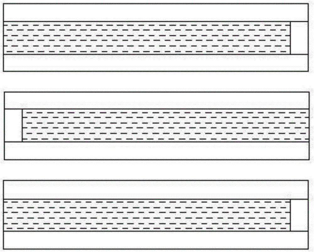
[0040] The hindering medium is selected from one of quartz tubes or ceramic tubes. The dimensions of the quartz tubes or ceramic tubes are as follows: outer diameter 2cm±1mm, inner diameter 1.8cm±0.1mm, length 500cm±1mm;
[0041] Coating a conductive layer on the inner wall of the quartz tube or ceramic tube, the thickness of the conductive coating is 0.01mm;
[0042] The inner wall of the above-mentioned quartz tube or ceramic tube is coated with a conductive layer by plasma sputtering, chemical deposition or metal powder sintering process. One end of the inner wall is completely coated with solder joints, and the other end is left blank with 4cm±1mm. See Figure 4 ;
[0043] The structure of the large-flow exhaust gas treatment medium-impeded discharge electrodes is arranged as follows: multiple parallel electrodes are arranged in a dislocation matrix, and three dielectric barrier...
PUM
| Property | Measurement | Unit |
|---|---|---|
| thickness | aaaaa | aaaaa |
| length | aaaaa | aaaaa |
| length | aaaaa | aaaaa |
Abstract
Description
Claims
Application Information
 - R&D
- Intellectual Property
- Life Sciences
- Materials
- Tech Scout
- Unparalleled Data Quality
- Higher Quality Content
- 60% Fewer Hallucinations
Browse by: Latest US Patents, China's latest patents, Technical Efficacy Thesaurus, Application Domain, Technology Topic, Popular Technical Reports.
© 2025 PatSnap. All rights reserved.Legal|Privacy policy|Modern Slavery Act Transparency Statement|Sitemap|About US| Contact US: help@patsnap.com


