Touch sensor substrate, touch panel, display device, and method for manufacturing touch sensor substrate

A touch sensor and touch panel technology, applied to instruments, conductive layers on insulating carriers, input/output processes of data processing, etc. The effect of visibility

Active Publication Date: 2019-08-13
VTS TOUCHSENSOR CO LTD
View PDF9 Cites 0 Cited by
  • Summary
  • Abstract
  • Description
  • Claims
  • Application Information

AI Technical Summary

Problems solved by technology

From the viewpoint of this translucency, the material for forming the electrode for position detection is preferably a transparent conductive material with high transparency such as ITO or ZnO. The greater the length of the electrode, the higher the resistance of the electrode itself and the lower the position detection sensitivity.

Method used


Image

  • Touch sensor substrate, touch panel, display device, and method for manufacturing touch sensor substrate
  • Touch sensor substrate, touch panel, display device, and method for manufacturing touch sensor substrate
  • Touch sensor substrate, touch panel, display device, and method for manufacturing touch sensor substrate

Examples


Embodiment 1

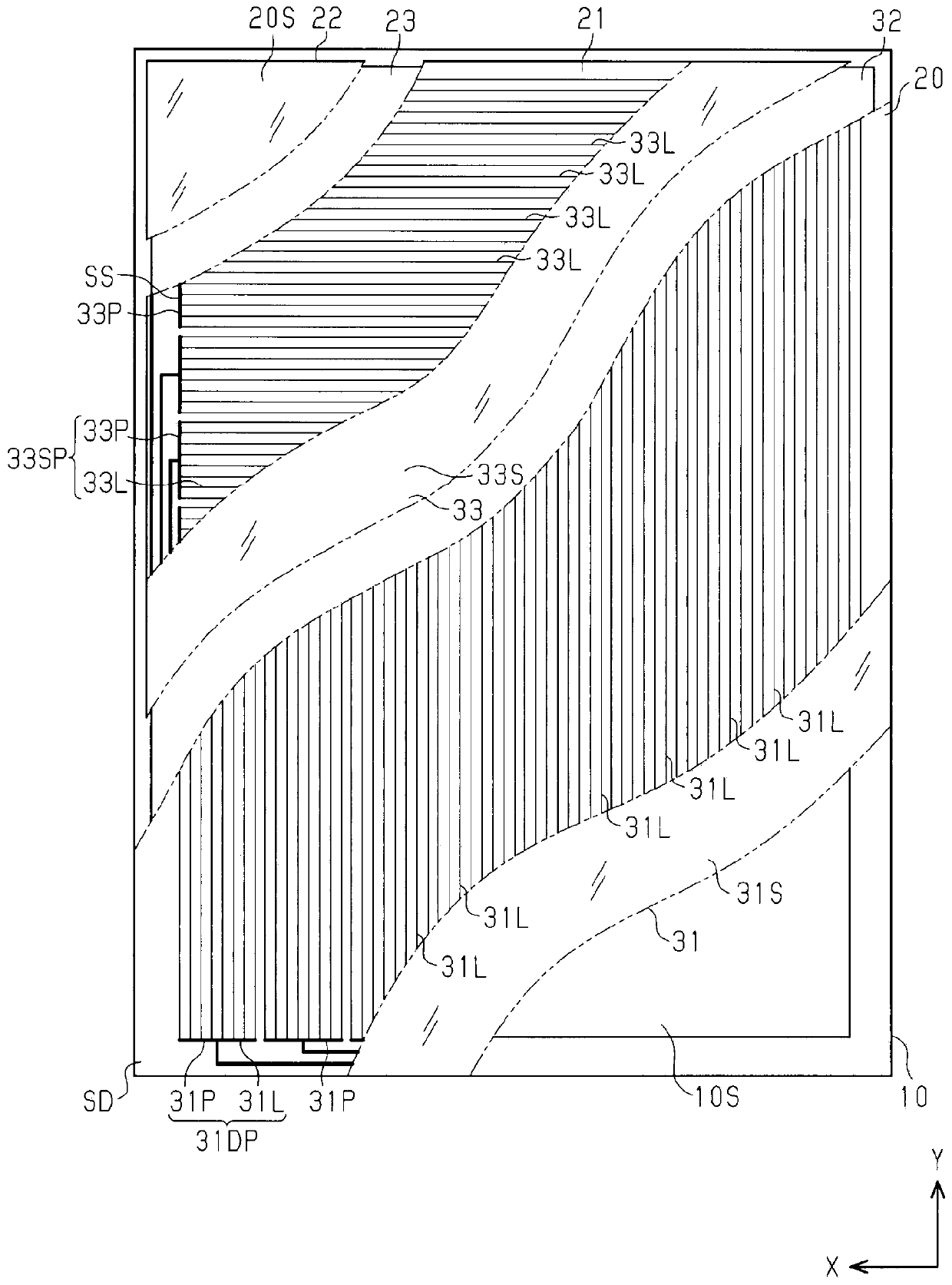
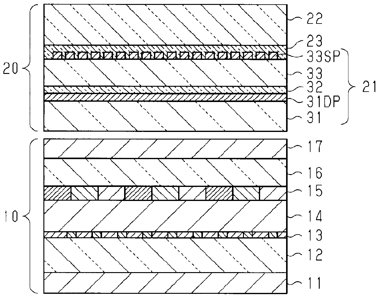
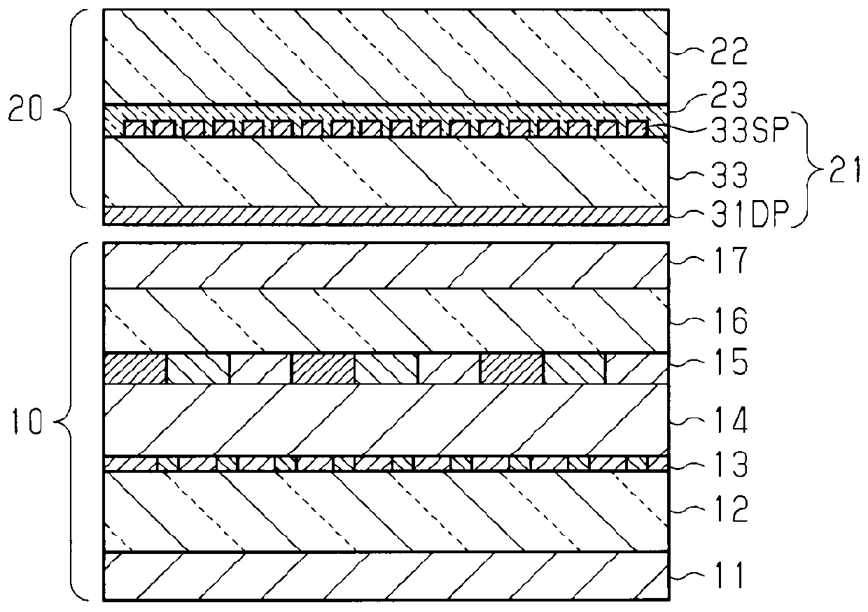
[0117] refer to Figure 12 (a) to (e) illustrate an embodiment of a method for manufacturing a touch sensor substrate. In addition, since the method of forming the first electrode 31DP is basically the same as the method of forming the second electrode 33SP, an example of obtaining a touch sensor substrate by forming the second electrode 33SP on the base material on which the second electrode 33SP is formed will be described below. in addition, Figure 12 In , an example of using PET with electrolytic copper foil bonded on one side and fabricating electrode groups arranged in stripes on PET by applying photolithography is described. However, the film formation method of the electrode pattern constituting the electrode group is not limited to foil paste.

[0118] like Figure 12 As shown in (a), a PET sheet with a thickness of 50 μm was used as the substrate.

[0119] like Figure 12 As shown in (b), an electrolytic copper foil 33R having a thickness of 3 μm was laminated ...

Embodiment 2

[0126] The blackening process of Example 1 was replaced with a substitution blackening process, and the conditions other than that were the same as Example 1, and the electrode which has the blackening layer BL of Example 2 was obtained. Specifically, copper on the surface of the copper electrode is substituted with palladium (Pd) to allow adhesion. At this time, the PET sheet on which the electrode pattern was formed was dipped in a hydrochloric acid solution containing Pd in ​​a range of 100 ppm to 500 ppm. Furthermore, when the color tone of the electrode pattern is changed to blue, the reflectance is less than 20% in the visible region (400nm to 780nm), and the surface resistivity is suppressed to 1Ω / □ or less. At this time, the thickness of the blackened layer BL is also about 0.2 μm. From this result, it can also be seen that from the viewpoint of reducing the increase in the resistance value of the electrode, the treatment time for performing the sulfurization treatmen...

Embodiment 3

[0133] The blackening treatment in Example 1 was changed to metal plating (Ni, Cr) treatment, and the conditions other than that were the same as in Example 1, and an electrode having a blackened layer BL in Example 3 was obtained. According to the electrode obtained by metal plating (Ni, Cr) treatment, compared with the electrode without blackening treatment, the reflectance in the visible region (400nm or more and 780nm or less) can be suppressed. As in Example 2, both the reflectance of less than 20% and the surface resistivity of 1Ω / □ or less are satisfied.


PUM


Abstract

The touch sensor substrate of the present invention includes a base material having a first electrode arrangement surface as an example of a first surface, and a first electrode as an example of a plurality of electrodes located on the first surface, and a plurality of the first electrodes Each has: a bottom surface in contact with the first surface; a top surface exposed from the first surface and facing the bottom surface; and a top surface exposed from the first surface and connecting the bottom surface and the top surface. The side surface, at least one of the bottom surface and the top surface, and the side surface are blackened layers BL.

Description

technical field [0001] The present invention relates to a touch sensor substrate including electrodes, a touch panel, a display device, and a method for manufacturing the touch sensor substrate. Background technique [0002] In recent years, touch sensors have been used in the operation parts of various electronic equipment represented by mobile phones, portable information terminals, ATMs, and car navigation systems. The touch sensor is attached to the display surface of an image display panel such as a liquid crystal display device as an input device for detecting a contact position of a fingertip or a pen tip. Touch sensors are classified into various types such as resistive film type, electrostatic capacitive type, optical type, and ultrasonic type according to the structure and detection method of the touch sensor, and are used according to the usage of electronic equipment. Among them, from the standpoint of excellent durability, transmittance, sensitivity, stability,...

Claims


Application Information

Patent Timeline
Patent Type & Authority Patents(China)
IPC IPC(8): G06F3/041G06F3/044
CPCG02F1/13338G06F3/0412G06F2203/04103G06F3/0445G06F3/0446H01B5/14G02F1/133502G02F1/134309G06F2203/04112G06F2203/04102G02F1/13439
Inventor 后藤宏希田中真纪中村玄
Owner VTS TOUCHSENSOR CO LTD
Why Eureka
Try Eureka