
Composite sheet for protective film formation

A technology of protective film and composite sheet, which is applied in the direction of film/sheet adhesive, semiconductor/solid-state device parts, semiconductor devices, etc., to achieve the effect of excellent laser transmittance and inhibition of adhesion

Active Publication Date: 2020-01-03
LINTEC CORP
View PDF15 Cites 0 Cited by
  • Summary
  • Abstract
  • Description
  • Claims
  • Application Information

AI Technical Summary

Problems solved by technology

Therefore, it becomes a structure in which the back side of the semiconductor chip on which no circuit is formed is exposed

Method used


Image

  • Composite sheet for protective film formation
  • Composite sheet for protective film formation
  • Composite sheet for protective film formation

Examples


Embodiment 1

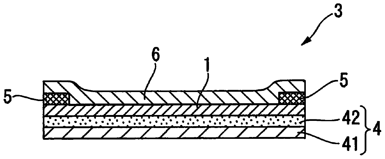
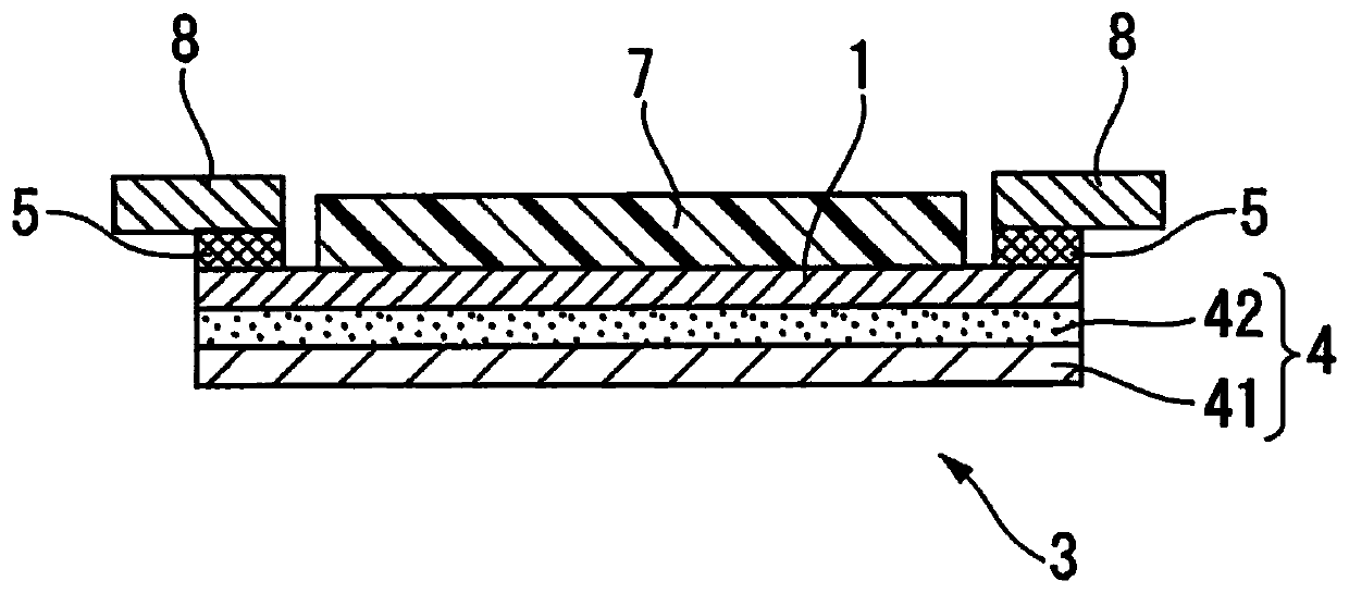
[0181] In Example 1, manufactured as follows image 3 , 4 The composite sheet 3 for forming a protective film is shown.

[0182] (1) Preparation of the first laminate including the protective film forming film

[0183] The following components were mixed in the compounding ratio (in terms of solid content) shown below, and diluted with methyl ethyl ketone so that the solid content concentration became 61% by mass to prepare a coating agent for forming a protective film.

[0184] (A) Adhesive polymer: 10 mass parts of n-butyl acrylate, 70 mass parts of methyl acrylate, 5 mass parts of glycidyl methacrylate and 15 mass parts of 2-hydroxyethyl acrylate (methyl acrylate) ) acrylate copolymer (weight average molecular weight: 800,000, glass transition temperature: -1°C) 100 parts by mass

[0185] (B-1) 60 parts by mass of bisphenol A epoxy resin (manufactured by Mitsubishi Chemical Corporation, jER828, epoxy equivalent 184 to 194 g / eq)

[0186] (B-2) 10 parts by mass of bisphen...

Embodiment 2~5 and comparative example 1~3

[0206] The arithmetic mean roughness (Ra1) and the arithmetic mean roughness (Ra2) after heating, the melting point, and the storage modulus at 130°C of the back surface of the substrate were changed as shown in Table 1 below, except Except that, the composite sheet for protective film formation of Examples 2-5 and Comparative Examples 1-3 was manufactured similarly to Example 1.


PUM

PropertyMeasurementUnit
surface roughnessaaaaaaaaaa
melting pointaaaaaaaaaa

Abstract

The protective film-forming composite sheet of the present invention is a protective film-forming composite sheet (3) comprising a support sheet (4) and a protective film-forming film (1) laminated on the first surface side of the support sheet (4), wherein , the arithmetic mean roughness (Ra1) of the second surface of the support sheet (4) is 0.2 μm or more, and the arithmetic mean of the second surface of the support sheet (4) after heating the support sheet (4) at 130°C for 2 hours The roughness (Ra2) is 0.25 μm or less.

Description

technical field [0001] The present invention relates to a composite sheet for forming a protective film capable of forming a protective film on a workpiece such as a semiconductor wafer, or forming a protective film on a processed product obtained by processing the workpiece (such as a semiconductor chip) . [0002] This application claims the priority of Japanese Patent Application No. 2014-106757 for which it applied in Japan on May 23, 2014, and uses the content here. Background technique [0003] In recent years, semiconductor devices have been manufactured using a mounting method called a face down method. In this method, when mounting a semiconductor chip having a circuit surface on which electrodes such as bumps are formed, the circuit surface side of the semiconductor chip is bonded to a chip mounting portion such as a lead frame. Therefore, there is a structure in which the back side of the semiconductor chip on which no circuit is formed is exposed. [0004] The...

Claims


Application Information

Patent Timeline
Patent Type & Authority Patents(China)
IPC IPC(8): H01L21/301C09J7/20C09J7/29C09J201/00H01L23/00
CPCC09J201/00H01L23/00H01L2924/0002C09J7/20H01L2924/00H01L21/324H01L21/6836H01L21/7806H01L24/28
Inventor 佐伯尚哉山本大辅米山裕之稻男洋一
Owner LINTEC CORP
Learn More