

Field effect transistor
A technology of field effect transistors and laminates, which is applied in the direction of transistors, semiconductor devices, semiconductor/solid state device manufacturing, etc., can solve the problems of uneven operation, insufficient suppression of ringing phenomenon and surge voltage, and inability to realize stable operation of field effect transistors and other problems, to achieve the effect of suppressing ringing phenomenon, suppressing surge voltage, and stabilizing work
- Summary
- Abstract
- Description
- Claims
- Application Information
AI Technical Summary
Problems solved by technology
Method used
Image

Examples
no. 1 approach
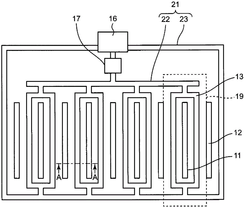
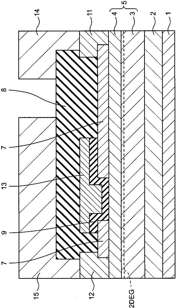
[0027] figure 1 It is a schematic plan view of a GaN-based HFET (Heterojunction Field Effect Transistor) according to the first embodiment of the present invention. figure 2 yes means figure 1 A sectional view of the A-A line section.
[0028] Such as figure 2 As shown, in the first embodiment, a buffer layer 2 , a GaN layer 3 and an AlGaN layer 4 are sequentially formed on a Si substrate 1 . The GaN layer 3 and the AlGaN layer 4 constitute a GaN-based laminated body 5 having a heterojunction. 2DEG (two-dimensional electron gas) is generated at the interface between the GaN layer 3 and the AlGaN layer 4 to form a channel. In addition, the aforementioned substrate is not limited to a Si substrate, and a sapphire substrate or a SiC substrate may also be used, and the GaN-based laminated body 5 may be grown on a sapphire substrate or a SiC substrate, or may be used, for example, on a GaN substrate. The GaN-based stacked body 5 is grown on a substrate made of a nitride se...
no. 2 approach
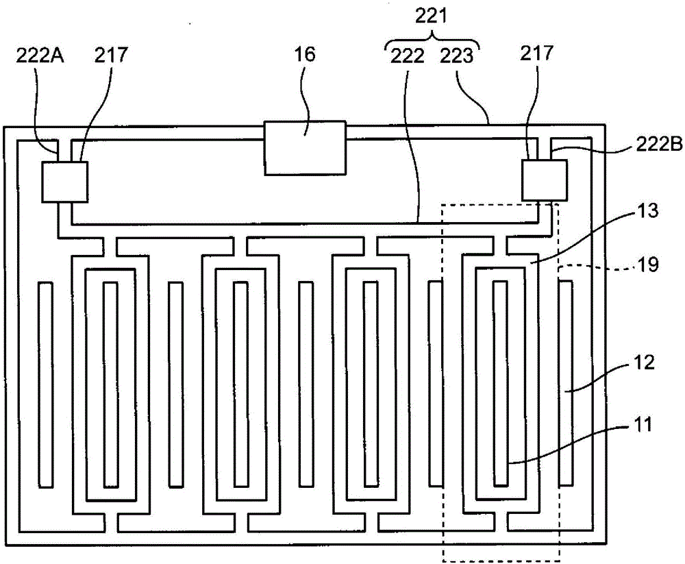
[0045] image 3 It is a schematic plan view of the GaN-based HFET of the second embodiment described above. The points different from the first embodiment described above will be described. In the second embodiment, resistive elements 217 and 217 are connected to the first wiring 222 of the gate electrode connection wiring 221 . In addition, in this second embodiment, the same reference numerals as in the above-mentioned first embodiment denote the same configurations as in the above-mentioned first embodiment, and description thereof will be omitted.
[0046] Such as image 3 As shown, both ends of the first wiring 222 of the gate electrode connecting wiring 221 are respectively connected to the gate electrode pad 16 via a part of the second wiring 223 of the gate electrode connecting wiring 221 . Resistive elements 217 and 217 are respectively connected to both ends 222A and 222B of the first wiring 222 . The sheet resistance values of the resistive elements 217 and 217...
no. 3 approach
[0049] Figure 4 It is a schematic plan view of the GaN-based HFET of the above-mentioned third embodiment. The difference from the above-mentioned first embodiment will be described. In this third embodiment, the first wiring 322 of the gate electrode connection wiring 321 is not connected to the resistance elements 217, 217, and both ends of the first wiring 322 Sections 322A, 322B constitute an impedance adjustment section. In addition, in this third embodiment, the same reference numerals as in the above-mentioned first embodiment denote the same configurations as in the above-mentioned first embodiment, and description thereof will be omitted.
[0050] Such as Figure 4 As shown, both ends of the first wiring 322 of the gate electrode connecting wiring 321 are respectively connected to the second wiring 323 of the gate electrode connecting wiring 321 . Both ends 322A, 322B of the first wiring 322 are bent and formed in a meandering manner. The CR time constant of the ...
PUM
 Abstract
Description
Claims
Application Information