
Substrate unit for power modules, and power module

A technology of power modules and substrates, which is applied in the direction of electrical components, circuits, and electric solid-state devices, can solve the problems that it is difficult to accurately locate multiple insulating substrates, it is difficult to obtain the position accuracy of insulating substrates, and it is difficult to achieve integration. Achieve high integration, improve connection reliability, and good heat dissipation

Active Publication Date: 2017-02-22
MITSUBISHI MATERIALS CORP
View PDF9 Cites 7 Cited by
  • Summary
  • Abstract
  • Description
  • Claims
  • Application Information

AI Technical Summary

Problems solved by technology

[0009] However, in the method described in Patent Document 1, even if good heat dissipation can be maintained by preventing cracking of the ceramic substrate and peeling of the encapsulating resin, a wiring member (lead frame) that is not too rigid must perform the positioning function. , so it is difficult to obtain the positional accuracy of each insulating substrate, and it is difficult to achieve higher integration
[0010] Also, as described in Patent Document 2, in the method of directly supporting the insulating substrates, it is not easy to accurately position a plurality of insulating substrates due to the limitation of the mold, etc.

Method used


Image

  • Substrate unit for power modules, and power module
  • Substrate unit for power modules, and power module
  • Substrate unit for power modules, and power module

Examples


Embodiment

[0088] Next, examples performed to confirm the effects of the present invention will be described.

[0089] As a sample of the substrate unit for a power module, a ceramic substrate composed of AlN with a thickness of 0.635 mm was prepared as a ceramic substrate layer, and a 0.6 mm-thick aluminum plate with a purity of 99.99 Aluminum plate with mass % or more (4N). Pass C1020 (yield strength = 195N / mm 2 ) or heat-resistant alloy ZC manufactured by Mitsubishi Shindoh Co., Ltd. (yield strength = 280N / mm 2 ), prepare plates with the thicknesses shown in Table 1. In addition, the value of yield strength is the value at room temperature (25 degreeC). The planar dimensions of each component were formed as shown in Table 1.

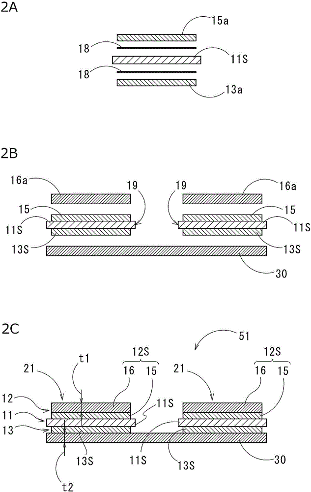
[0090] These were joined by the joining method described in the said embodiment, and the sample of the board|substrate unit for power modules was produced. "Embodiment" in Table 1 indicates which embodiment of the production method each sample was produced ...


PUM


Abstract

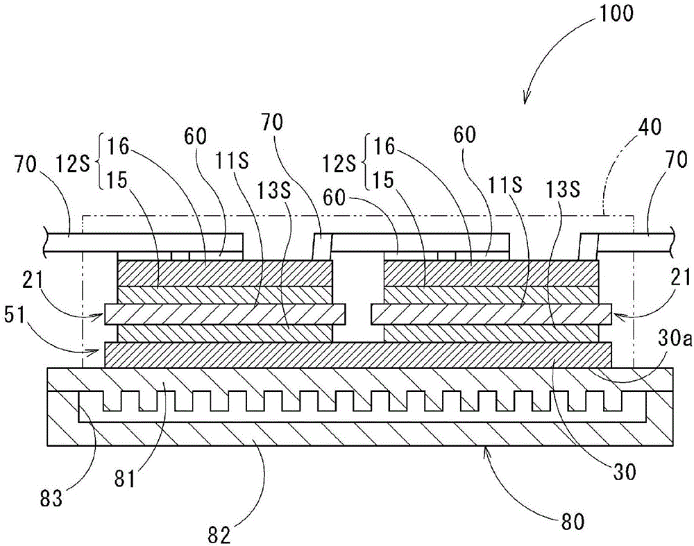
A substrate unit (51) for power modules, wherein: a circuit layer (12) is configured of a plurality of small circuit layers (12S); a ceramic substrate layer (11) is configured of at least one sheet; and a metal layer (13) is configured of at least one sheet. Each small circuit layer (12S) has a multilayer structure that comprises a first aluminum layer (15) which is bonded to one surface of the ceramic substrate layer (11) and a first copper layer (16) which is bonded to the first aluminum layer (15) by solid-phase diffusion. The metal layer (13) is formed of the same material as the first aluminum layer (15). A heat dissipation plate (30) is formed of copper or a copper alloy, and the metal layer (13) and the heat dissipation plate (30) are bonded to each other by solid-phase diffusion. If t1 (mm) is the thickness of the first copper layer (16), A1 (mm<2>) is the bonded area of the first copper layer (16), sigmate1 (N / mm<2>) is the proof stress of the first copper layer (16), t2 is the thickness of the heat dissipation plate (30) at the position where the heat dissipation plate (30) is bonded to the metal layer, A2 (mm2) is the bonded area of the heat dissipation plate (30) at the above-described position and sigmate2 (N / mm<2>) is the proof stress of the heat dissipation plate (30) at the above-described position, the ratio (t1* A1*sigmate1) / (t2* A2*sigmate<2>) is from 0.80 to 1.20 (inclusive).

Description

technical field [0001] The present invention relates to a power module substrate unit and a power module used in semiconductor devices that control large current and high voltage. [0002] This application claims priority based on Japanese Patent Application No. 2014-138716 filed on July 4, 2014 and Japanese Patent Application No. 2015-130972 filed on June 30, 2015, and uses the contents thereof here. Background technique [0003] The power module uses a substrate for a power module in which a metal plate forming a circuit layer is bonded to one side of a ceramic substrate including aluminum nitride, and a heat sink is bonded to the other side. A semiconductor element such as a power element is mounted on a circuit layer of the power module substrate via a solder material. [0004] The miniaturization of semiconductor elements has been promoted with the increase in output density, and the integration of modules has been increasingly demanded. As a general integration of po...

Claims


Application Information

Patent Timeline
IPC IPC(8): H01L23/13H01L23/36H01L25/07H01L25/18
CPCH01L2224/40137H01L23/36H01L25/18H01L23/3735H01L25/072H01L2224/37147C04B37/026H01L23/3731H01L23/3736H01L23/4334H01L23/473C04B2237/121C04B2237/402C04B2237/407C04B2237/706C04B2237/86C04B35/645C04B2237/343C04B2237/366C04B2237/368C04B2237/66C04B2237/704
Inventor 大井宗太郎大开智哉
Owner MITSUBISHI MATERIALS CORP
Learn More