Novel electronic tag production process

A technology of electronic tags and production technology, which is applied in the direction of recording carriers used in machines, instruments, computer parts, etc., can solve the problems of RFID technology application range limitation, label chip and antenna disconnection, epoxy resin damage, etc., to meet the requirements of large The effect of mass production, remarkable effect, and ingenious design ideas

Inactive Publication Date: 2017-03-08
SHANGHAI BIZGRID INFORMATION TECH
View PDF8 Cites 4 Cited by
  • Summary
  • Abstract
  • Description
  • Claims
  • Application Information

AI Technical Summary

Problems solved by technology

Some high-temperature-resistant materials such as PPA can not deform at 300°C, and can indeed protect the connection between the chip and the antenna from damage in a short period of time. However, if the tag is kept at 300°C for too long, the surface temperature of the electronic tag will still reach the same temperature. The epoxy or conductive glue protecting the bonding point will be damaged and cause the tag chip to disconnect from the antenna and fail
[0007] In addition, adding plastic shell materials to the high-temperature-resistant ceramic materials, silicon chips, and metal wires will greatly increase the overall cost, which will greatly limit the application range of RFID technology.

Method used


Image

  • Novel electronic tag production process
  • Novel electronic tag production process
  • Novel electronic tag production process

Examples


Embodiment 1

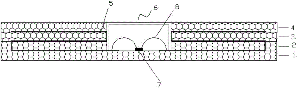
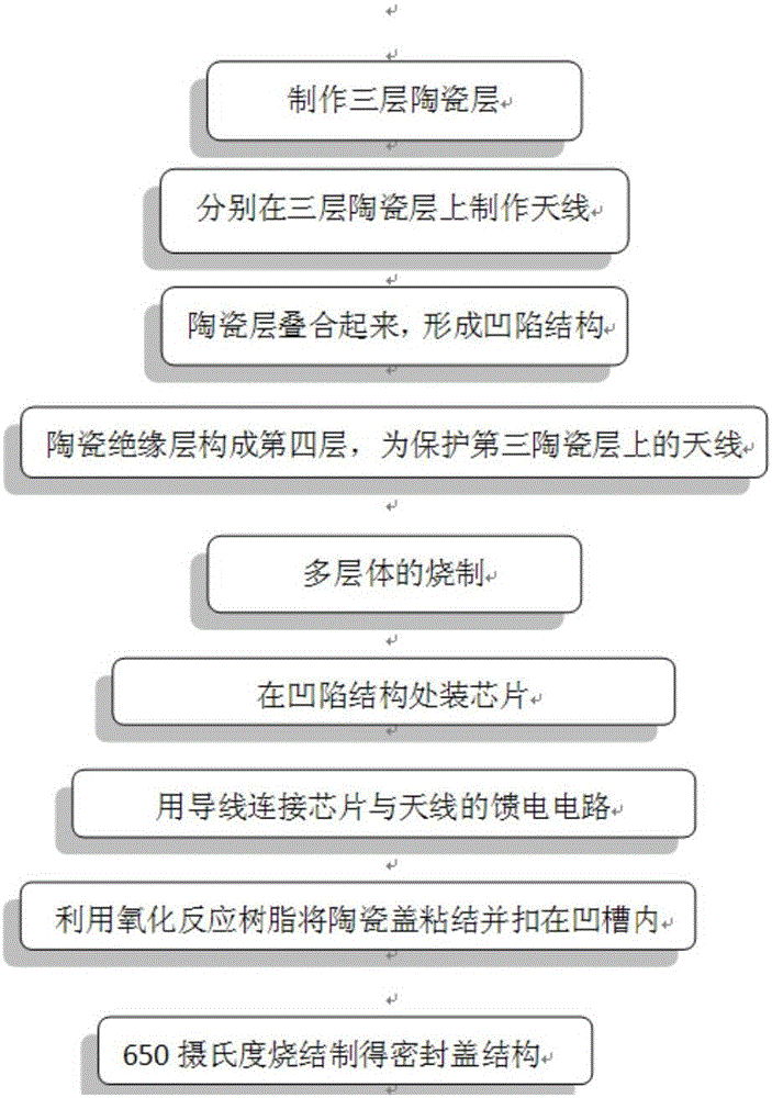
[0024] Such as figure 1 , image 3 As shown, the specific production process of ceramic RFID is as follows:

[0025] 1) Make three ceramic layers

[0026] 2) Make the antenna on the ceramic layer respectively

[0027] 3) The multilayer body with groove structure composed of three layers of ceramic layer, antenna and ceramic insulating layer is fired into the antenna substrate

[0028] 4) Put the IC chip into the groove structure of the antenna substrate, and use conventional prior art methods to bind the IC chip to the feed antenna circuit of the antenna in the groove

[0029] 5) Buckle the cover of the ceramic material on the groove structure of the substrate, and the contact part is pre-coated with oxidation reaction glue

[0030] 6) High temperature firing into RFID

Embodiment 2

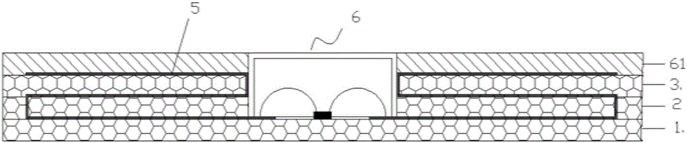
[0032] This embodiment 2 is an alternative to embodiment 1, and the final product is as figure 2 shown. refer to image 3 The flow shown in this embodiment is adjusted to:

[0033] The specific production process of ceramic RFID is as follows:

[0034] 1) Make three ceramic layers

[0035] 2) Make the antenna on the ceramic layer respectively

[0036] 3) The multilayer body with groove structure composed of ceramic layer and antenna is fired into the antenna substrate

[0037] 4) Put the IC chip into the groove structure of the antenna substrate, and use conventional prior art methods to bind the IC chip to the feed antenna circuit of the antenna in the groove

[0038] 5) Buckle the cover 6 of ceramic material on the groove structure of the substrate, the outer part of the cover 6 has a ceramic edge structure, and the contact with the substrate is pre-coated with oxidation reaction glue

[0039] 6) Firing into RFID at high temperature to obtain the whole integrated cera...


PUM


Abstract

The invention discloses a novel electronic tag production process, which comprises the following steps of step 1.sintering and curing a printed antenna and a substrate to form an antenna substrate through the existing conventional process; step 2.placing an IC chip into a groove structure of the antenna substrate and adopting the existing conventional technical method to bind the IC chip on a feeding point of the antenna in the groove without epoxy resin dripping protection; step 3.providing a ceramic cover; step 4.bucklling the cover in the step 3 on the groove structure of the substrate and pre-coating oxidizing reaction glue on a contact place, wherein the IC chip is arranged in the cover, and two sides of the cover are ends of the antenna, which are used for adjusting a tag frequency band; and step 5.sintering at high temperature (the field is usually within the range of 600-700 DEG C), and reacting and sintering the oxidizing reaction to make the ceramic cover and the ceramic substrate form a whole body on the groove structure and form a closed space. A product obtained by the process of the invention is suitable for various high and low temperature application environments.

Description

technical field [0001] The invention relates to a preparation process of an electronic label of radio frequency identification technology. Background technique [0002] Traditional chip and RFID antenna binding methods include: FLIP CHIP (inverted packaging), wire bonding (WIRE Bonding), SMT reflow wave soldering. [0003] FLIP CHIP (upside-down packaging) uses asynchronous conductive adhesive in all directions, and realizes the connection between the chip pin and the antenna through extruded metal balls, and the cured conductive adhesive in other places provides overall support. However, the conductive adhesive will also be denatured and damaged at high temperatures exceeding 250°C, resulting in connection failure. [0004] Wire bonding (WIRE Bonding): Use gold wire or aluminum wire to connect the chip pin and the bonding point of the antenna. The epoxy resin dripped onto the chip wraps the chip and wires like amber, and after drying at 180°C, the cured epoxy resin glue p...

Claims


Application Information

Patent Timeline
Patent Type & Authority Applications(China)
IPC IPC(8): G06K19/077
CPCG06K19/07745
Inventor 王刚
Owner SHANGHAI BIZGRID INFORMATION TECH
Why Eureka
Try Eureka