Flexible circuit board and manufacturing method thereof

A technology of flexible circuit boards and manufacturing methods, which is applied in the fields of flexible printed circuit boards, printed circuit manufacturing, multilayer circuit manufacturing, etc., can solve problems such as monopoly and high material costs, and achieve the goal of reducing production costs and signal transmission losses Effect

Inactive Publication Date: 2017-03-08
AVARY HLDG (SHENZHEN) CO LTD +2
View PDF5 Cites 8 Cited by
  • Summary
  • Abstract
  • Description
  • Claims
  • Application Information

AI Technical Summary

Problems solved by technology

In addition, Teflon and liquid crystal polymers are special materials with high material costs, and have even been monopolized by major material suppliers.

Method used


Image

  • Flexible circuit board and manufacturing method thereof
  • Flexible circuit board and manufacturing method thereof
  • Flexible circuit board and manufacturing method thereof

Examples


Embodiment Construction

[0043] The flexible circuit board and the manufacturing method of the flexible circuit board provided by the present invention will be described in detail below in combination with specific embodiments.

[0044] The manufacturing method of the flexible circuit board 100 provided by the present invention includes the following steps.

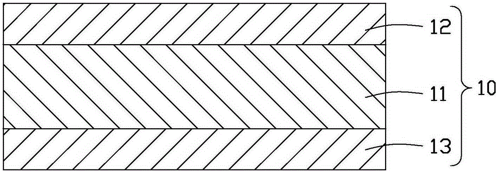
[0045] For a first step, see figure 1 , providing a first copper clad substrate 10 .

[0046] In this embodiment, the first copper clad substrate 10 is a double-sided flexible copper foil substrate. The first copper clad substrate 10 includes a first base material layer 11 , a first copper foil layer 12 and a first outer copper foil layer 13 . The first substrate layer 11 is located between the first copper foil layer 12 and the first outer copper foil layer 13 .

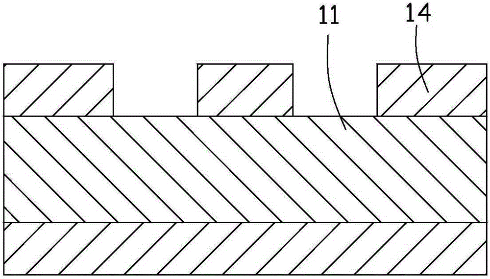
[0047] In the second step, see figure 2 and Figure 9 , making the first copper foil layer 12 to form the conductive circuit layer 14 .

[0048] The conductive circuit layer 14 ...


PUM


Abstract

The invention relates to a flexible circuit board, which comprises a base material layer, a conductive circuit layer, a film and a second base material layer, wherein the first base material layer and the second base material layer are located at two opposite sides of the conductive circuit layer; the second base material layer is bonded with the conductive circuit layer through the film; the conductive circuit layer comprises at least one linear signal line, at least two ground lines and at least two hollow areas; the ground lines and the linear signal lines are alternately arranged; each hollow area is located between one linear signal line and one ground line; a first opening corresponding to the linear signal lines and the hollow areas at two sides thereof is formed in the film; and the first opening communicates with the hollow areas to form an air barrier layer surrounding the linear signal lines. The invention further relates to a manufacturing method of the flexible circuit board.

Description

technical field [0001] The invention relates to a printed circuit board technology, in particular to a flexible circuit board and a method for manufacturing the flexible circuit board. Background technique [0002] With the development of electronic signal transmission towards high frequency and high speed, the electronic industry has increasingly stringent requirements for signal transmission loss. Signal transmission loss mainly includes wire loss and dielectric loss. During the transmission of high-frequency signals, the dielectric loss is greater than the wire loss. The dielectric loss is positively correlated with the dielectric loss factor and the relative dielectric constant. Traditional signal transmission structures usually use Teflon (Teflon), Liquid Crystal Polyester (LCP) or other pure glue with low dielectric constant as the dielectric layer to reduce insertion loss. However, both Teflon and liquid crystal polymers still have high dielectric constants. For ex...

Claims


Application Information

Patent Timeline
Patent Type & Authority Applications(China)
IPC IPC(8): H05K1/02H05K3/46
CPCH05K1/0218H05K3/4635H05K2201/05H05K1/0219H05K2201/0154H05K1/024H05K1/189H05K3/4697H05K2201/0715H05K2201/09618H05K2201/09809H01P3/003H01P3/085H01P11/003H05K3/4652
Inventor 胡先钦沈芾云罗鉴何明展庄毅强
Owner AVARY HLDG (SHENZHEN) CO LTD
Why Eureka
Try Eureka