semiconductor device
A semiconductor, conductive type technology, applied in the direction of semiconductor devices, electrical components, circuits, etc., can solve the problem of increasing on-resistance, and achieve the effect of improving on-resistance and withstand voltage
- Summary
- Abstract
- Description
- Claims
- Application Information
AI Technical Summary
Problems solved by technology
Method used
Image


Examples
no. 1 approach
[0020] The semiconductor device according to this embodiment includes: a semiconductor layer having a first surface and a second surface; a drift region of the first conductivity type provided in the semiconductor layer; and a first conductive type drift region provided in the semiconductor layer between the drift region and the first surface. The body region of the second conductivity type; the source region of the first conductivity type of the semiconductor layer disposed between the body region and the first surface; the first gate electrode; sandwiching the body region between the first gate electrode and the first gate electrode the second gate electrode provided; the first gate insulating film provided between the first gate electrode and the body region; the second gate insulating film provided between the second gate electrode and the body region; A first field plate electrode between the second surface and the first gate electrode; a second field plate electrode dispo...
no. 2 approach
[0075] The semiconductor device of this embodiment is the same as that of the first embodiment except that it does not include the first insulating film and the second insulating film. Therefore, descriptions of contents overlapping with those of the first embodiment are omitted.
[0076] Figure 6 It is a schematic cross-sectional view of the semiconductor device of this embodiment. The semiconductor device 200 of the present embodiment is a vertical MOSFET including a gate electrode in a trench.
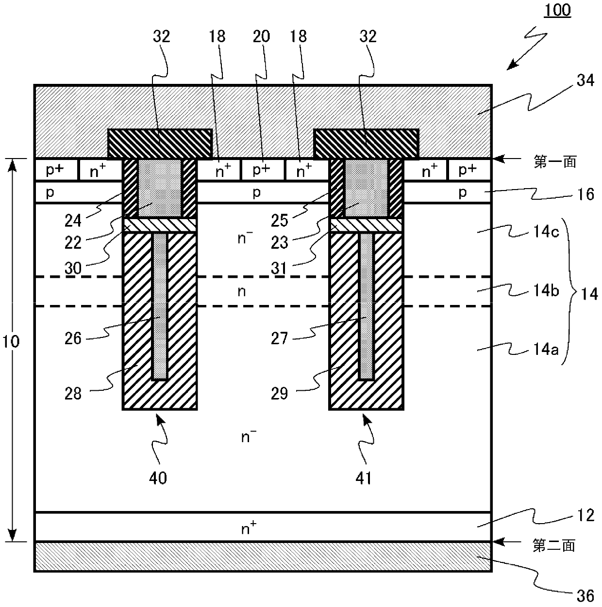
[0077] The MOSFET 200 of this embodiment includes a silicon layer (semiconductor layer) 10 . Silicon layer 10 has n + type of drain region 12, n - Type or n-type drift region 14, p-type body region 16, n + type source region 18 and p + type of body contact region 20 . Drift zone 14 has n - Type lower region (first region) 14a, n-type middle region (second region) 14b, n - Type upper region (third region) 14c.
[0078] Furthermore, MOSFET 200 includes a first gate electrod...
PUM
 Abstract
Description
Claims
Application Information
 - R&D
- Intellectual Property
- Life Sciences
- Materials
- Tech Scout
- Unparalleled Data Quality
- Higher Quality Content
- 60% Fewer Hallucinations
Browse by: Latest US Patents, China's latest patents, Technical Efficacy Thesaurus, Application Domain, Technology Topic, Popular Technical Reports.
© 2025 PatSnap. All rights reserved.Legal|Privacy policy|Modern Slavery Act Transparency Statement|Sitemap|About US| Contact US: help@patsnap.com