OLED display device package and packaging method
A display device and packaging method technology, which is applied in the manufacture of electric solid-state devices, semiconductor devices, semiconductor/solid-state devices, etc., can solve the problem that the water and oxygen barrier performance cannot fully meet the needs of large-size OLED display devices, and achieve the improvement of mechanical properties and Adhesive performance, blocking moisture and oxygen, and preventing corrosion
- Summary
- Abstract
- Description
- Claims
- Application Information
AI Technical Summary
Problems solved by technology
Method used
Image


Examples
Embodiment approach 1
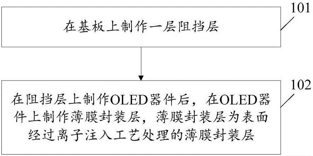
[0072] The structure of the OLED display device package made in this embodiment is as follows: figure 2 shown, combined with figure 2 , this embodiment includes the following steps:
[0073] In the first step, a barrier layer 30 is formed on the flexible substrate 10. The barrier layer 30 includes an inorganic thin film layer, an organic thin film layer and a surface-modified inorganic thin film layer; the surface-modified inorganic thin film layer is surface-treated by an ion implantation process The inorganic thin film layer includes an inorganic thin film layer and an ion implantation layer injected into the surface of the inorganic thin film layer.
[0074] In the second step, an inorganic thin film layer 31 , an organic thin film layer 32 and an inorganic thin film layer 33 a are sequentially deposited on the OLED device 20 (cathode) prepared on the barrier layer 30 .
[0075] The third step is to use ion implantation technology to implant ions on the surface of the i...
Embodiment approach 2
[0078] The structure of the OLED display device package made in this embodiment is as follows: image 3 shown, combined with image 3 , this embodiment includes the following steps:
[0079] In the first step, a barrier layer 40 is formed on the flexible substrate 10, and the barrier layer includes a surface-modified inorganic thin film layer, a surface-modified organic thin film layer and a surface-modified inorganic thin film layer. The surface modified inorganic thin film layer includes an inorganic thin film layer and an ion implantation layer injected into the surface of the inorganic thin film layer; the surface modified organic thin film layer includes an organic thin film layer and an ion implantation layer injected into the surface of the organic thin film layer; the surface modified inorganic thin film layer includes an inorganic thin film layer. A thin film layer and an ion implantation layer implanted into the surface of the inorganic thin film layer.
[0080]In ...
Embodiment approach 3
[0085] The structure of the OLED display device package made in this embodiment is as follows: Figure 4 shown, combined with Figure 4 , this embodiment includes the following steps:
[0086] In the first step, ions are implanted on the flexible substrate 10a for surface modification, and a smooth and dense ion-implanted layer 10b is formed on the surface of the flexible substrate 10a.
[0087] In the second step, a barrier layer 50 is formed on the modified flexible substrate 10. The barrier layer 50 includes an inorganic thin film layer, an organic thin film layer and a surface modified inorganic thin film layer; the surface modified inorganic thin film layer includes an inorganic thin film layer and a surface modified inorganic thin film layer. The ion implantation layer implanted into the surface of the inorganic thin film layer.
[0088] In the third step, an inorganic thin film layer 51 , an organic thin film layer 52 and an inorganic thin film layer 53 a are sequenti...
PUM
 Abstract
Description
Claims
Application Information