Cerenkov radiation device and manufacturing method thereof, and radiation extraction method

A radiation device and device technology, applied in the field of Cerenkov radiation device, extraction of Cerenkov radiation, and preparation, can solve problems that need to be improved and are difficult to meet the requirements of practical applications

Active Publication Date: 2017-04-19
TSINGHUA UNIV
View PDF6 Cites 9 Cited by
  • Summary
  • Abstract
  • Description
  • Claims
  • Application Information

AI Technical Summary

Problems solved by technology

However, the above-mentioned Cerenkov radiation devices are difficult to meet the requirements of many practical applications in terms of realization conditi

Method used


Image

  • Cerenkov radiation device and manufacturing method thereof, and radiation extraction method
  • Cerenkov radiation device and manufacturing method thereof, and radiation extraction method
  • Cerenkov radiation device and manufacturing method thereof, and radiation extraction method

Examples


Embodiment 1

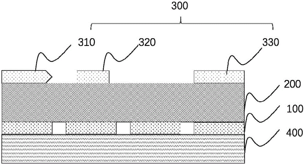
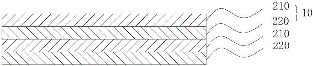
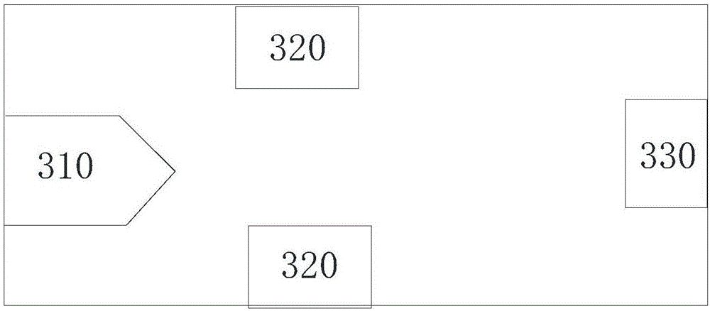
[0067] Au is used to form the metal periodic nano-slit structure, wherein the Au film thickness is 100nm, the slit period is 800nm, and the duty ratio is 0.12. The hyperbolic metamaterial structure adopts the dielectric-conductor alternating multilayer film form, in which the conductor is Au and the dielectric is SiO 2 . The production process is as follows: first grow a layer of SiO on the already fabricated metal periodic nano-slit structure 2 As an isolation layer, this SiO 2 The layer thickness is about 50 nm. Next, by magnetron sputtering method on SiO 2 A layer of Au film was grown on the surface of the layer with a thickness of 10nm. Repeat this process to alternately grow 10nm SiO 2 and 10nm Au, a total of 20 layers of films were produced for ten cycles. The metal used is Mo to prepare the electron emission source, and a layer of SiO is first grown 2 As an isolation layer, the thickness is about 40nm, as an insulating isolation layer, and then make the electrode...

Embodiment 2

[0069] Al is used to form a metal periodic nano-slit structure, wherein the Al film thickness is 100nm, the slit period is 300nm, and the duty ratio is 0.12. The hyperbolic metamaterial structure adopts the dielectric-conductor alternating multilayer film form, in which the conductor is Al and the dielectric is SiO 2 . The production process is as follows: first grow a layer of SiO on the already fabricated metal periodic nano-slit structure 2 As an isolation layer, this SiO 2 The layer thickness is about 10 nm. Next, by magnetron sputtering method on SiO 2 A layer of Al film was grown on the surface of the layer with a thickness of 10nm, and then a layer of SiO was sputtered 2 film with a thickness of 10 nm. Repeat this process to alternately grow 10nm Al and 10nm SiO 2 , making a total of twenty layers of film ten cycles. The metal used is Mo to prepare the electron emission source, and a layer of SiO is first grown 2 As an isolation layer, the thickness is about 30n...

Embodiment 3

[0071] Au is used to form the metal periodic nano-slit structure, in which the Au film thickness is 100 nm, the slit period is 300 μm, and the duty ratio is 0.12. The hyperbolic metamaterial structure adopts the form of dielectric-conductor alternating multilayer film, in which the conductor is graphene and the dielectric is Si. The production process is as follows: first grow a layer of SiO on the already fabricated metal periodic nano-slit structure 2 As an isolation layer, this SiO 2 The layer thickness is about 50 nm. Next, transfer about 0.3nm graphene to SiO by graphene transfer technology 2 Layer surface, and then use sputtering method to prepare a layer of Si film with a thickness of 15nm. Repeat this process, alternately transfer 0.3nm graphene and grow 15nm Si, and make a total of 20 layers of films for ten cycles. The metal used is Mo to prepare the electron emission source, and a layer of SiO is first grown 2 As an isolation layer, the thickness is about 40nm,...


PUM

PropertyMeasurementUnit
Thicknessaaaaaaaaaa
Thicknessaaaaaaaaaa
Thicknessaaaaaaaaaa

Abstract

The invention discloses a Cerenkov radiation device and a manufacturing method thereof, and a radiation extraction method. The Cerenkov radiation device comprises a metal cycle nanometer slit structure, a hyperbolic metamaterial structure and an electron-emitting source, wherein the hyperbolic metamaterial structure is arranged on an upper surface of the metal cycle nanometer slit structure; the electron-emitting source is arranged on an upper surface of the hyperbolic metamaterial structure; and the electron-emitting source includes an anode, a cathode and a grid electrode. The Cerenkov radiation device does not need a high voltage. A characteristic that a phase velocity of light in the hyperbolic metamaterial structure can be reduced by several orders of magnitudes compared to a velocity in a traditional material is used so that a required electronic flight speed generated by Cerenkov radiation can be greatly reduced; and then production cost generated by the Cerenkov radiation device is decreased and safety performance is increased.

Description

technical field [0001] The invention relates to the field of semiconductors, in particular to a Cerenkov radiation device, a preparation method and a method for extracting Cerenkov radiation. Background technique [0002] Cherenkov radiation (Cherenkov Radiation, CR) is a kind of electromagnetic radiation produced when the speed of flying charged particles is greater than the phase speed of light in the surrounding medium. Cerenkov radiation plays an important role in many fields of science. Cerenkov radiation sources have the advantages of high power and large spectrum range. The research on various Cerenkov radiation devices has attracted many researchers around the world. In biomedicine, biological tissue labeled with radioactive elements produces charged particles that excite Cerenkov radiation in the organism, which can be used for the detection of labeled cells. In experimental physics, particle counters designed according to the principle of Cherenkov radiation are ...

Claims


Application Information

Patent Timeline
IPC IPC(8): G01T1/22
CPCG01T1/22
Inventor 刘仿肖龙王梦轩黄翊东张巍冯雪崔开宇
Owner TSINGHUA UNIV
Why Eureka
Try Eureka