Method for forming fin field effect transistor

A fin field effect tube and fin technology, which is applied to semiconductor devices, electrical components, circuits, etc., can solve the problems that the electrical performance of fin field effect tubes needs to be improved, and achieve improved electrical performance, good feature size and morphology Effect

Active Publication Date: 2017-04-19
SEMICON MFG INT (SHANGHAI) CORP +1
View PDF4 Cites 13 Cited by
  • Summary
  • Abstract
  • Description
  • Claims
  • Application Information

AI Technical Summary

Problems solved by technology

[0005] However, the electrical performance of the fin field effect transistor formed by the prior art needs to be improved

Method used


Image

  • Method for forming fin field effect transistor
  • Method for forming fin field effect transistor
  • Method for forming fin field effect transistor

Examples


Embodiment Construction

[0032] It can be seen from the background art that the electrical performance of the fin field effect transistor formed in the prior art needs to be improved.

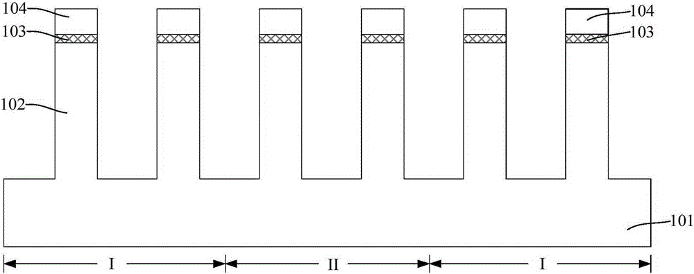
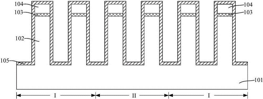
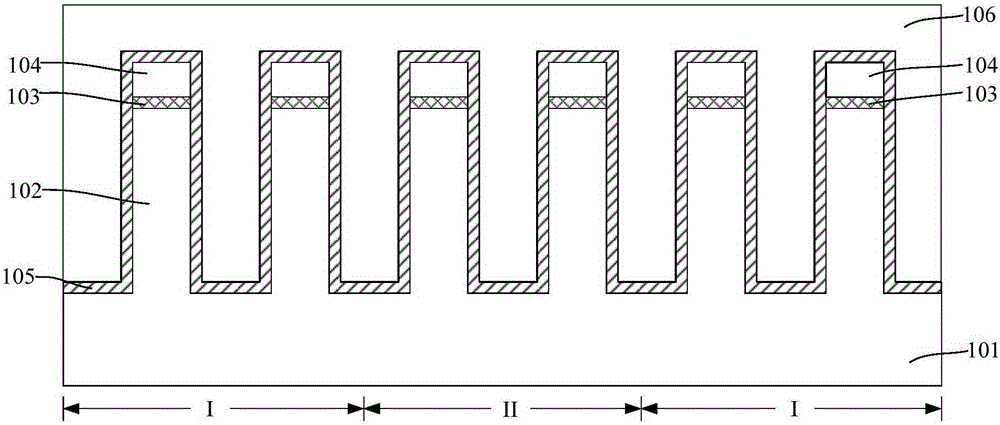
[0033] It has been found through research that the pattern density of each region of the substrate is not completely the same. According to the pattern density of the substrate surface, the substrate can include a pattern-dense area (Dense Area) and a pattern-sparse area (ISO Area). The pattern density of the fins located on the substrate surface of the dense area is greater than the pattern density of the fins located on the substrate surface of the sparse area.

[0034] The process steps of forming the fins include: providing an initial substrate including a sparse area and a dense area; forming a patterned mask layer on the surface of the initial substrate, and openings are formed in the patterned mask layer, wherein, The opening size in the mask layer above the sparse area is larger than the opening size in the mas...


PUM


Abstract

A method for forming a fin field effect transistor comprises: providing a substrate, wherein the substrate includes first regions and second regions located between adjacent first regions, a plurality of discrete fins are formed on the surface of the substrate, and the distances between the adjacent fins are the same; fully filling the surface of the substrate between the adjacent fins with a first dielectric layer, wherein the first dielectric layer covers the sidewall surfaces of the fins; removing the first dielectric layer of the second regions to expose the sidewall surfaces of the fins in the second regions; oxidizing the fins of the second regions to convert the fins of the second regions into an oxidizing structure; forming a second dielectric layer on the substrate in the second regions, wherein the second dielectric layer also covers the sidewall surface of the oxidizing structure, and the sidewall surface of the first dielectric layer in the first regions; etching back a part of thickness of the first dielectric layer, the second dielectric layer, and the oxidizing structure. The method forms a number of fins with different pattern densities and with good feature sizes and morphology so as to improve the electrical performance of the fin field effect transistor.

Description

technical field [0001] The invention relates to the technical field of semiconductor manufacturing, in particular to a method for forming a fin field effect transistor. Background technique [0002] With the continuous development of semiconductor process technology, the development trend of semiconductor process nodes following Moore's Law continues to decrease. In order to adapt to the reduction of process nodes, the channel length of MOSFET field effect transistors has to be continuously shortened. The shortening of the channel length has the advantages of increasing the die density of the chip and increasing the switching speed of the MOSFET field effect tube. [0003] However, as the channel length of the device is shortened, the distance between the source and the drain of the device is also shortened, so that the control ability of the gate to the channel becomes worse, and the gate voltage pinches off the channel. The difficulty is also increasing, making the pheno...

Claims


Application Information

Patent Timeline
Patent Type & Authority Applications(China)
IPC IPC(8): H01L21/8234H01L29/66
CPCH01L29/66795H01L21/823412H01L21/823431H01L21/823481
Inventor 赵海
Owner SEMICON MFG INT (SHANGHAI) CORP
Why Eureka
Try Eureka