Check patentability & draft patents in minutes with Patsnap Eureka AI!

Array substrate and AMOLED display apparatus

An array substrate and substrate technology, applied in electrical components, electrical solid devices, circuits, etc., can solve problems such as component damage of AMOLED display devices, and achieve the effect of reducing the probability of component damage, reducing the overlapping area, and reducing the impact.

Active Publication Date: 2017-04-26
WUHAN CHINA STAR OPTOELECTRONICS TECH CO LTD
View PDF8 Cites 4 Cited by
  • Summary
  • Abstract
  • Description
  • Claims
  • Application Information

AI Technical Summary

Problems solved by technology

[0005] In the process of using the above-mentioned AMOLED display device, the inventors of the present invention found that since a plurality of the data lines DL' are electrically connected to the driving circuit through the surface metal block 110, the connection between the surface metal block 110 and the data line DL' There is an insulating layer between them, thereby forming a parasitic capacitance, which will have an impact on the resistance-capacitance delay (RCDelay) of the transmission of the signal on the data line DL'; A large amount of static electricity will be accumulated during the manufacturing process, and electrostatic discharge (ESD) will cause damage to the components of the AMOLED display device

Method used


Image

  • Array substrate and AMOLED display apparatus
  • Array substrate and AMOLED display apparatus
  • Array substrate and AMOLED display apparatus

Examples


no. 1 example

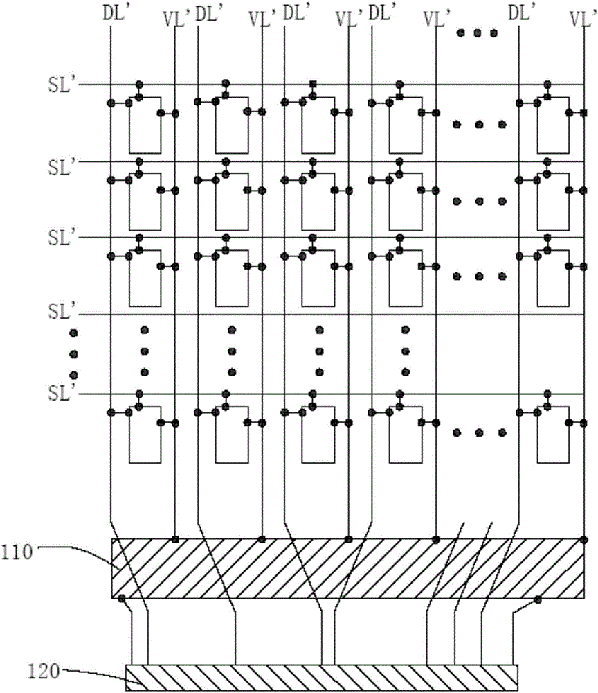
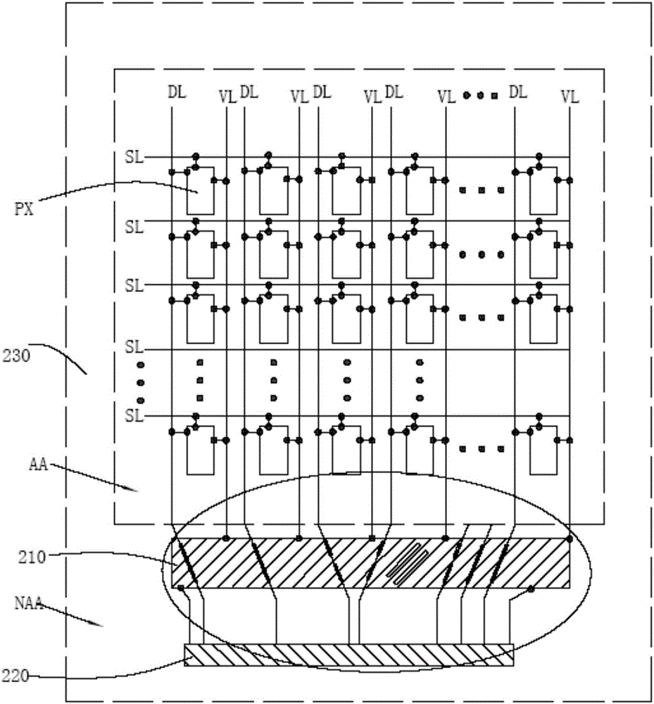
[0039] Please refer to Figure 2-Figure 4 An AMOLED (Active Matrix OLED, active matrix organic light emitting diode) display device provided by an embodiment of the present invention includes an array substrate and a thin film encapsulation layer, and the thin film encapsulation layer is located above the array substrate. The array substrate includes a substrate 230 , a driver chip 220 , a plurality of data lines DL, a plurality of high level lines VL and a surface metal block 210 .

[0040]The substrate 230 can be a rigid substrate, such as a glass substrate, or a flexible substrate, such as a polyimide plastic substrate. The driving chip 220 is located on the substrate 230 , and in this embodiment, the driving chip 220 is located on the lower side of the substrate 230 . A plurality of the data lines DL are sequentially arranged on the substrate 230, and extend longitudinally to be electrically connected with the driver chip 220. The chip 220 is electrically connected, that...

no. 2 example

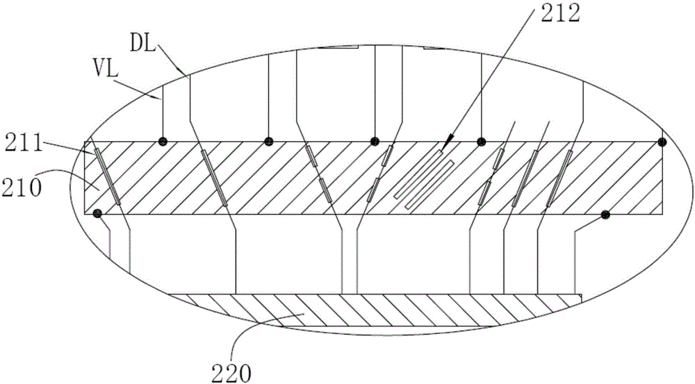
[0051] Figure 5 An array substrate provided in the second embodiment of the present invention, Figure 5 structure with figure 2 The structures are similar, so the same element symbols represent the same elements. The main difference between this embodiment and the first embodiment is the surface metal block.

[0052] See Figure 5 and Image 6, in this embodiment, the hollowed out area is a large opening 311, and the opening 311 straddles at least two of the data lines DL, for example, the opening 311 straddles two of the data lines DL, three The data lines DL, four data lines DL, five data lines DL, six data lines DL, ten data lines DL, twenty data lines DL, thirty data lines DL or across all data lines DL. Specifically, in this embodiment, the opening 311 is rectangular, and the rectangular opening 311 extends from the left side of the surface metal block 310 to the right side of the surface metal block 310, and extends from the upper side of the surface metal block ...


PUM


Abstract

The embodiment of the invention discloses an array substrate. The array substrate comprises a substrate, a driving chip located on the substrate, a plurality of data lines arranged on the substrate in sequence, a plurality of high-level lines, and a surface metal block located on the substrate and electrically connected with the plurality of high-level lines, the data lines vertically extend to be electrically connected with the driving chip, the plurality of high-level lines are located in the same high level, the plurality of data lines pass through an area which the surface metal block is located in and are electrically connected with the driving chip, an insulating layer is arranged between the surface metal block and the plurality of data lines, and overlapping positions of the surface metal block and the data lines are provided with hollow areas to reduce the parasitic capacitance formed by the surface metal block and the data lines. The embodiment of the invention also discloses an AMOLED display apparatus. By employing the array substrate and the AMOLED apparatus, the influence of capacitance-resistance delay is reduced, and the damage to components is reduced.

Description

technical field [0001] The invention belongs to the field of display technology, and in particular, relates to an array substrate and an AMOLED display device. Background technique [0002] Organic light emitting diode (Organic Light Emitting Display, OLED) display device has self-illumination, low driving voltage, high luminous efficiency, short response time, high definition and contrast, nearly 180° viewing angle, wide operating temperature range, and can realize flexible display and With many advantages such as large-area full-color display, it is recognized by the industry as a display device with the most potential for development. [0003] OLED display devices can be divided into passive matrix OLED (Passive Matrix OLED, PMOLED) display devices and active matrix OLED (Active Matrix OLED, AMOLED) display devices according to the driving method, namely direct addressing and thin film transistor ( Thin Film Transistor, TFT) matrix addressing two types. Among them, the ...

Claims


Application Information

Patent Timeline
Patent Type & Authority Applications(China)
IPC IPC(8): H01L27/32
CPCH10K59/12H10K59/131H01L27/0288H01L27/124
Inventor 陈彩琴
Owner WUHAN CHINA STAR OPTOELECTRONICS TECH CO LTD
Features
  • R&D
  • Intellectual Property
  • Life Sciences
  • Materials
  • Tech Scout
  • Unparalleled Data Quality
  • Higher Quality Content
  • 60% Fewer Hallucinations
Learn More