
zno conductive covariant substrate vertical structure type gan ultraviolet led

A vertical structure, LED chip technology, applied in the direction of circuits, electrical components, semiconductor devices, etc., can solve the problems of difficult large-scale application, poor conductivity, high price, etc., and achieve the effect of low cost, controllable conductivity and cost saving

Active Publication Date: 2019-03-19
NANJING UNIV
View PDF5 Cites 0 Cited by
  • Summary
  • Abstract
  • Description
  • Claims
  • Application Information

AI Technical Summary

Problems solved by technology

At present, the concentration of Li, Na and other impurities in the 2-inch ZnO single crystal prepared by Jingbo Company of Japan and Cermet of the United States is as high as 10 16 cm -3 , due to poor conductivity due to inability to dope, the price is relatively expensive, and my country is blocked on large-size substrates
At present, the Fujian Institute of Physical Structure of the Chinese Academy of Sciences and the Shanghai Institute of Optics and Mechanics can prepare ZnO single crystals of about 1 inch, but the quality and size of the crystals still have a certain gap with foreign countries, which makes ZnO bulk single crystals comparable to self-supporting GaN substrates. Advantages can be said, so it is difficult to apply on a large scale

Method used


Image

  • zno conductive covariant substrate vertical structure type gan ultraviolet led
  • zno conductive covariant substrate vertical structure type gan ultraviolet led

Examples


Embodiment Construction

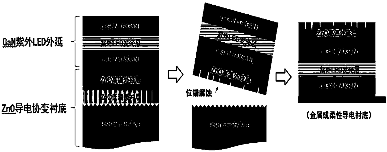
[0013] The present invention proposes a ZnO conductive covariant substrate vertical structure type GaN ultraviolet LED structure, and the present invention is further described through specific process steps below:

[0014] (1) Using PSS sapphire as the substrate, use MOCVD and other processes to grow ZnO low-temperature buffer layer and ZnO high-temperature epitaxial layer to form a ZnO conductive covariant substrate, grow GaN ultraviolet LED epitaxy on this substrate, and optimize the growth of ZnO low-temperature buffer layer The temperature is about 450-480°C, and the growth temperature of ZnO high-temperature epitaxial layer is 850-1000°C;

[0015] (2) Using diluted HCl aqueous solution, the stripping of the ZnO covariant substrate GaN ultraviolet LED chip from the sapphire substrate is realized by chemical etching;

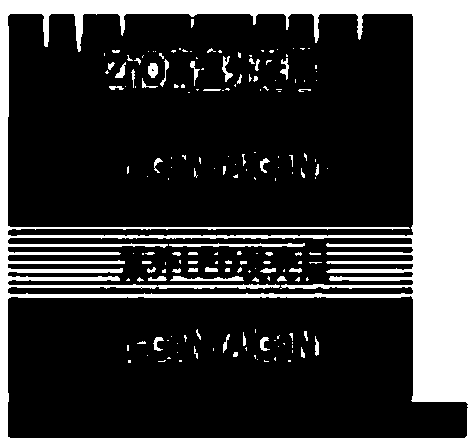
[0016] (3) After peeling off, the flip-chip LED chips can be transferred to metal and flexible substrates to form vertical GaN UV LEDs.

[0017] Compared w...


PUM


Abstract

A ZnO conductive covariant substrate vertical structure type GaN UV LED uses a nano-pattern (PPS) sapphire as an epitaxial substrate, uses a MOCVD method to grow a ZnO low temperature buffer layer and a ZnO high temperature epitaxial layer, uses a ZnO epitaxial layer as a high quality conductive substrate, a GaN UV LED epitaxial is formed in a following step, and an LED chip is peeled and transferred, thus forming the ZnO conductive covariant substrate vertical structure type GaN UV LED. The novel vertical structure type GaN UV LED can reduce the device cost, and can improve the luminous efficiency of the GaN UV LED. The ZnO conductive covariant substrate vertical structure type GaN UV LED is simple in peeling technology, low in cost, and can be applied to the flexible substrate luminous project.

Description

technical field [0001] The invention relates to the preparation of LEDs, in particular to a ZnO conductive covariant substrate vertical structure type GaN ultraviolet LED structure and its preparation process, belonging to the technical field of semiconductor lighting. Background technique [0002] The improvement of the luminous efficiency of ultraviolet LED has always been a hot spot that people pay attention to. To improve luminous efficiency, it is the general trend to develop power-type ultraviolet LED devices, among which vertical structure chips are currently the mainstream technology route adopted by power-type LEDs. For the manufacture of LED chips, the selection of substrate materials is the primary consideration, and power devices put forward higher requirements for the conductivity and thermal conductivity of substrate materials. [0003] The most common substrate for GaN growth is Al 2 o 3 , which has the advantages of good chemical stability, no absorption o...

Claims


Application Information

Patent Timeline
Patent Type & Authority Patents(China)
IPC IPC(8): H01L33/02H01L33/00
CPCH01L33/0093H01L33/02
Inventor 叶建东张彦芳沈洋卞岳任芳芳朱顺明汤琨顾书林
Owner NANJING UNIV
Learn More