Quantum dot display panel and manufacturing method thereof

A display panel and quantum dot technology, which is applied in semiconductor/solid-state device manufacturing, electrical components, circuits, etc., can solve problems such as increasing production costs, affecting device performance, and color mixing, so as to avoid easy color mixing and improve device performance.

Active Publication Date: 2017-04-26
TCL CORPORATION
View PDF4 Cites 21 Cited by
  • Summary
  • Abstract
  • Description
  • Claims
  • Application Information

AI Technical Summary

Problems solved by technology

[0005] In view of the above-mentioned deficiencies in the prior art, the object of the present invention is to provide a quantum dot display panel and a manufacturing method thereof, aiming at solving the problem that the removal of the residual pixel bank layer in the existing method will affect the performance of later devices, and the process of removing the residual pixel bank layer It will increase the production cost and the problem of easy color mixing

Method used


Image

  • Quantum dot display panel and manufacturing method thereof
  • Quantum dot display panel and manufacturing method thereof
  • Quantum dot display panel and manufacturing method thereof

Examples


Embodiment Construction

[0025] The present invention provides a quantum dot display panel and a manufacturing method thereof. In order to make the purpose, technical solution and effect of the present invention clearer and clearer, the present invention will be further described in detail below. It should be understood that the specific embodiments described here are only used to explain the present invention, not to limit the present invention.

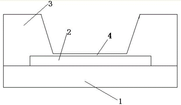
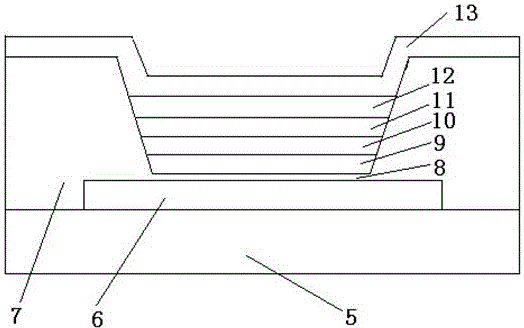
[0026] see figure 2 , figure 2 It is a schematic structural diagram of a preferred embodiment of a quantum dot display panel of the present invention. As shown in the figure, the quantum dot display panel sequentially includes a substrate 5, a pixel electrode 6 located in the pixel electrode pattern area of ​​the substrate, and a pixel The pixel bank layer 7 in the electrode peripheral area, the pixel bank layer 8 remaining on the pixel electrode 6 , the electron transport layer 9 , the quantum dot light emitting layer 10 , the hole transport layer 11 , ...


PUM


Abstract

The invention discloses a quantum dot display panel and manufacturing method thereof. The quantum dot display panel includes a substrate, a pixel electrode located in a substrate pixel electrode pattern region, a pixel bank layer in a peripheral region of the pixel electrode, a residual pixel bank layer on the pixel electrode, an electron transport layer, a quantum dot luminous layer, a hole transport layer, a hole injection layer and an anode layer in sequence from bottom to top. A residual bank film on the pixel electrode during pixel bank manufacture is used as an electron blocking layer, a QLED of an inverted structure is manufactured, due to an insulating characteristic of the bank film, charge injection of the pixel electrode to the QLED device is reduced, thereby achieving electron and hole injection balance in the QLED, improving device performance, at the same time, the problem of removing the residual bank film and the problem of easy color mixing caused by the process can also be avoided, the manufacturing cost is reduced, and the yield is improved.

Description

technical field [0001] The invention relates to the technical field of displays, in particular to a quantum dot display panel and a manufacturing method thereof. Background technique [0002] Semiconductor quantum dots have excellent characteristics such as high light color purity, high luminous quantum efficiency, adjustable luminous color, and long service life. These characteristics make quantum dot light-emitting diodes (QLEDs) with quantum dot materials as the light-emitting layer have broad application prospects in solid-state lighting, flat panel display and other fields, and have attracted extensive attention from academia and industry. [0003] In recent years, through the improvement of quantum dot material synthesis process and the optimization of device structure, the performance of QLED has been greatly improved. However, due to the deep energy level of quantum dot material, it is difficult to inject holes and easy to inject electrons, resulting in carrier Imba...

Claims


Application Information

Patent Timeline
Patent Type & Authority Applications(China)
IPC IPC(8): H01L51/50H01L51/52H01L51/56
CPCH10K50/115H10K50/18H10K50/86H10K2102/321H10K71/00
Inventor 陈亚文
Owner TCL CORPORATION
Why Eureka
Try Eureka