General bias circuit board for aerospace semiconductor device total dose radiation test

A technology of total dose radiation and bias circuit, applied in the direction of single semiconductor device testing, measuring electricity, measuring device, etc., can solve the evaluation speed that restricts the radiation resistance of the device, the irradiation bias circuit board cannot be used with each other, the circuit board The effective radiation area is not large, so as to achieve the effect of improving the reusable rate, improving the effective utilization rate, and flexible splitting

Active Publication Date: 2017-05-10
CHINA ACADEMY OF SPACE TECHNOLOGY
View PDF5 Cites 6 Cited by
  • Summary
  • Abstract
  • Description
  • Claims
  • Application Information

AI Technical Summary

Problems solved by technology

[0004] However, most of the bias circuit boards used in the total dose test at home and abroad are individually designed test circuit boards according to the static bias power-on state of different devices. Different devices have different pin definitions and different power-on conditions. state, so that the irradiation bias circuit boards of different devices cannot be used with each other, and one bias circuit board can only be used for the total dose test of one device, resulting in low utilization rate of the bias circuit board and high test cost; In addition, each device must be independently designed and manufactured with a bias circuit board, resulting in a long test cycle for the total dose, which seriously restricts the evaluation speed of the device's radiation resistance. For the rapidly developing aerospace industry, this situation needs to be improved urgently
In addition, besides the devices and fixtures that need to be irradiated, there are also some resistors and capacitors required by the bias circuit on the bias circuit board produced at home and abroad. These resistance-capacitance components occupy a lot of space on the bias circuit board. , so that the effective radiation area of ​​the circuit board is not large, and due to the limitation of the uniformity of the radiation field of the cobalt source, the irradiation area with the same dose rate is limited. All test devices above, these are very unfavorable under the current machine-time conditions with limited radiation sources

Method used


Image

  • General bias circuit board for aerospace semiconductor device total dose radiation test
  • General bias circuit board for aerospace semiconductor device total dose radiation test
  • General bias circuit board for aerospace semiconductor device total dose radiation test

Examples


Embodiment Construction

[0025] Attached below Figure 1-4 The present invention is described in further detail with specific embodiment:

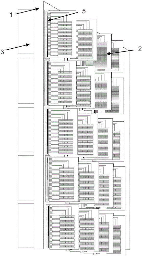
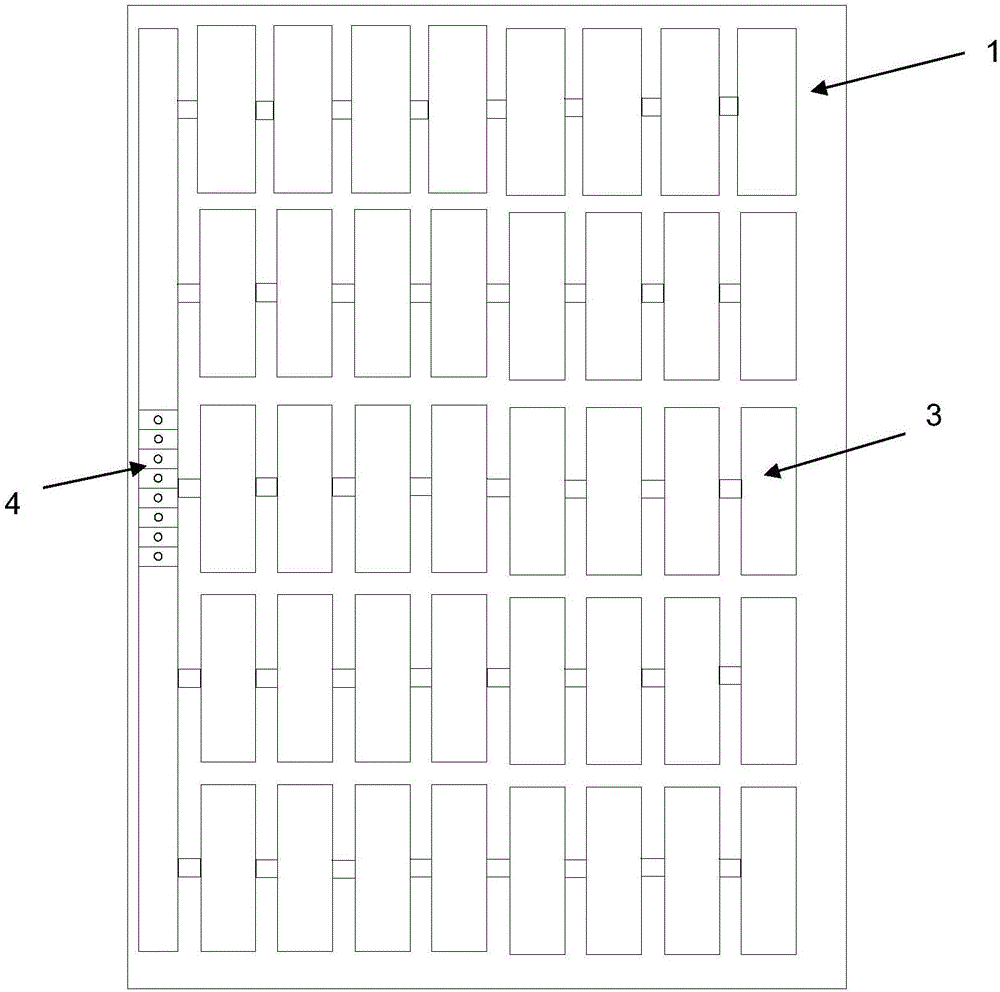
[0026] The outline structure of the general bias circuit board is as follows: figure 1 As shown, the general bias circuit board for the total dose radiation test of semiconductor devices used in aerospace is mainly composed of three parts: a motherboard 1, a general daughter board 2 and a test device fixture 3, and both the mother board 1 and the general daughter board 2 are PCB boards (printed circuit board), there are N motherboard slots 5 that are not connected to each other on the motherboard 1, and the universal daughter board is vertically inserted into the motherboard slots.

[0027] The motherboard front side structure of the universal bias circuit board is as follows figure 2 As shown, the motherboard 1 is used to provide multiple independent power supplies for the irradiation device. Motherboard card slot 5 includes power connection points and device...


PUM


Abstract

The invention discloses a general bias circuit board for aerospace semiconductor device total dose radiation test. The general bias circuit board comprises a motherboard, multiple general daughter boards independent of one another, and multiple test device fixtures. The general daughter boards are used for configuring voltages and bias loads for different irradiated devices, and are vertically inserted onto the back of the motherboard. The test device fixtures are used for inserting the irradiated devices, and are arranged on the front of the motherboard in a centralized way. For devices which are packaged in the same way and different in pin definition and power-on bias, total dose radiation test can be completed using the same motherboard by configuring different general daughter boards. For devices which are packaged in different ways and are the same in pin definition and power-on bias, total dose radiation test can be completed using the same motherboard by welding different test device fixtures. The space of the motherboard occupied by resistive and capacitive components is reduced, and the effective radiation area is increased effectively. Moreover, the general bias circuit board has the advantages of easy fabrication, low cost, high efficiency, reusability and high universality, and has popularization and application values.

Description

technical field [0001] The invention relates to a circuit board used for a total dose radiation test, in particular to a general bias circuit board used for a total dose radiation test of aerospace components, belonging to the field of total dose radiation tests of aerospace semiconductor devices. Background technique [0002] In the current space environment, there is a total dose radiation effect, and in order for the spacecraft to work normally in the complex space environment, it is necessary to strengthen the design of the spacecraft against the radiation effect. In the process of reinforcement design, it is necessary to give the anti-radiation ability index of semiconductor devices, so it is first necessary to evaluate the anti-radiation ability of semiconductor devices for aerospace, and to carry out ground total dose simulation experiments for aerospace components to obtain the anti-radiation ability of semiconductor devices for aerospace. Total dose irradiation capa...

Claims


Application Information

Patent Timeline
Patent Type & Authority Applications(China)
IPC IPC(8): G01R31/26
CPCG01R31/2607
Inventor 吕贺罗磊张洪伟于庆奎
Owner CHINA ACADEMY OF SPACE TECHNOLOGY
Why Eureka
Try Eureka