Dual-band visible light broadband absorption structure and preparation method thereof

An absorption structure and visible light technology, applied in optics, optical components, instruments, etc., can solve the problems of sensitivity to incident light angle, complex design structure, and inability to mass-produce, and achieve high absorption efficiency, wide application, and high absorption efficiency. small effect

Active Publication Date: 2017-05-10
SVG TECH GRP CO LTD +1
View PDF7 Cites 6 Cited by
  • Summary
  • Abstract
  • Description
  • Claims
  • Application Information

AI Technical Summary

Problems solved by technology

[0007] The problems existing in the above-mentioned prior art are: (1) Most of the designed structures are too complex, the preparation process is difficult, and it cannot be mass-produced; (2) In order to achieve polarization insensitivity, most

Method used


Image

  • Dual-band visible light broadband absorption structure and preparation method thereof
  • Dual-band visible light broadband absorption structure and preparation method thereof
  • Dual-band visible light broadband absorption structure and preparation method thereof

Examples


Embodiment approach

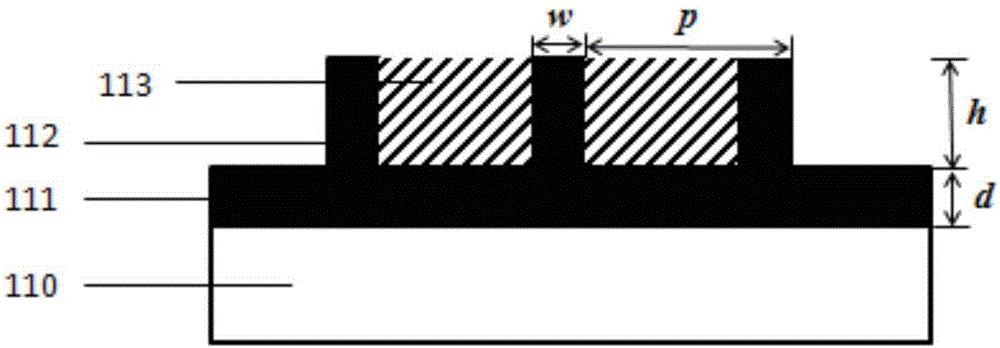
[0068] The cross-sectional structure of a dual-band visible light broadband absorbing structure involved in an embodiment of the present invention is as follows: figure 1 As shown, it includes a substrate 110 , a metal layer 111 , a metal grating layer 112 and a filling medium 113 . Wherein, the material of the base 110 is a transparent flexible material, such as polyester (PET), polycarbonate (PC), polyvinyl chloride (PVC), polymethyl methacrylate (PMMA) or polypropylene (BOPP). The metal layer 111 is located on the substrate 110 and its material is, for example, aluminum, silver, copper, tungsten, nickel, chromium or titanium. The metal layer 111 acts as a reflector. In order to ensure light reflection efficiency, the thickness d of the metal layer 111 is greater than the skin depth of visible light on the metal material. In one embodiment, the thickness of the metal layer 111 is 100nm. The metal grating layer 112 is located on the metal layer 111 and its material is, for ...

Embodiment 1

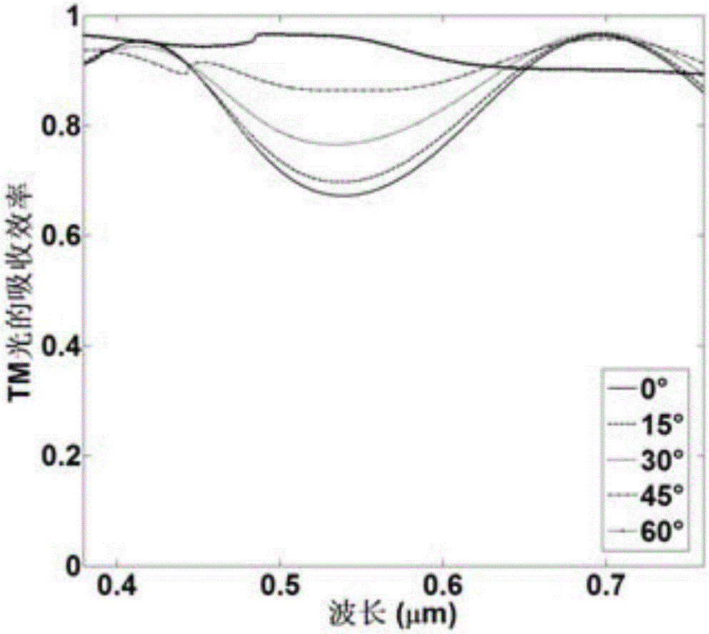
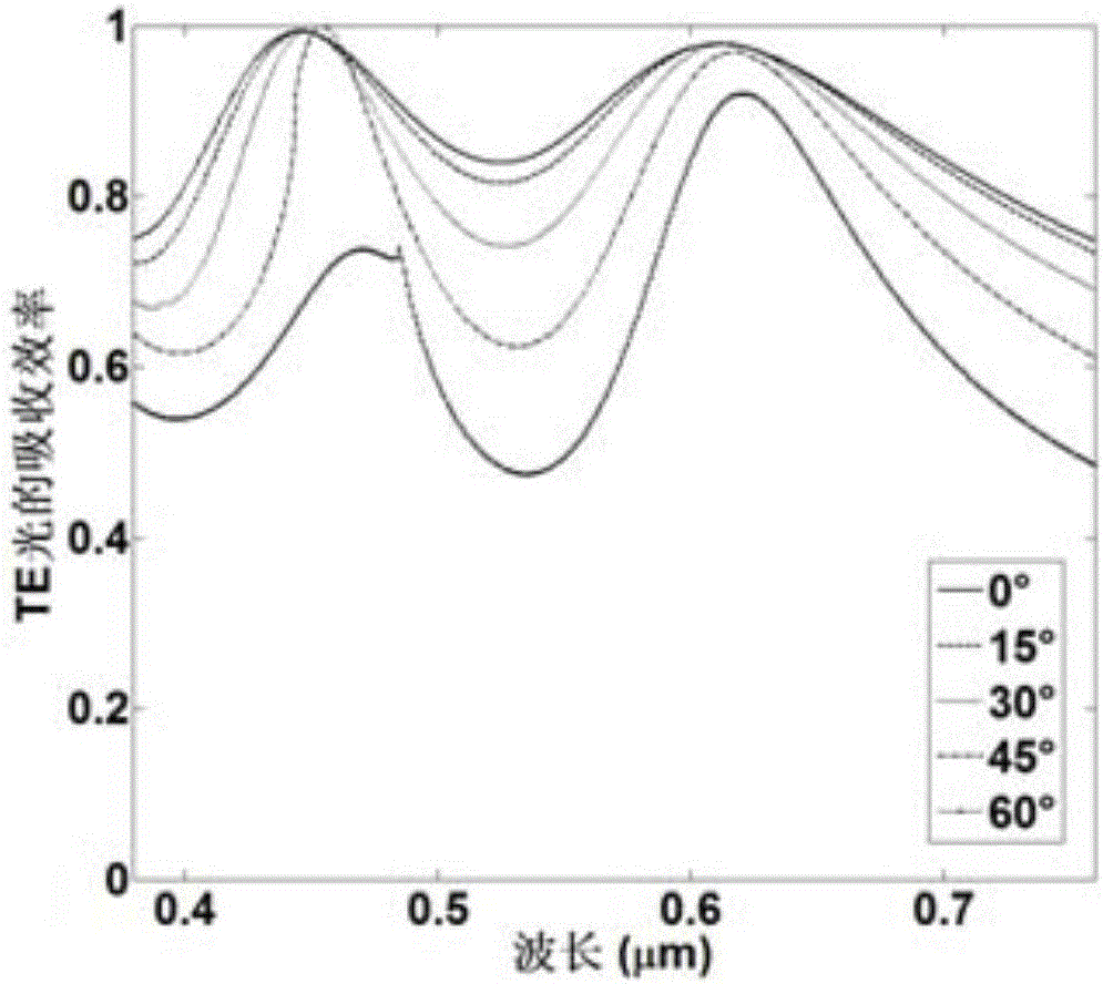
[0072] figure 2 and image 3 The relationship between the absorption spectrum of TM polarized light and TE polarized light of the broadband absorbing structure designed for the present invention, incident angle and incident wavelength. Wherein, p is 260nm, f is 0.25, h is 300nm, d is 100nm, the material of the metal layer and the metal grating layer is nickel, and the filling medium is silicon dioxide. The absorption characteristics and angle tolerance of broadband absorbing structures are analyzed by rigorous coupled wave theory (RCWA). Due to the coupling of surface plasmons excited by TM polarized light in the medium, a strong magnetic field resonance is formed to realize light energy capture, resulting in high-efficiency absorption. The mechanism of high absorption of TE polarized light lies in the formation of an open cavity between the filling medium and the metal walls on both sides, and the high absorption caused by cavity resonance. It can be found that both TM an...

Embodiment 2

[0074] Figure 4 and Figure 5 The relationship diagrams of the absorption spectra of the TM polarized light and the TE polarized light of the visible light broadband absorption structure with the period of the metal grating layer and the incident wavelength are respectively shown. In this embodiment, the period p of the metal grating is adjusted, and the influence of the change of p on the absorption spectrum of the structure is observed. Other structural parameters are the same as those in Embodiment 1, and the incident angle is 0 degree. It can be found that the period variation has a great influence on the TM light absorption, and preferably, the absorption bandwidth near the period of 250 nm is large and the efficiency is high. Period has little effect on TE polarized light.


PUM

PropertyMeasurementUnit
Heightaaaaaaaaaa
Thicknessaaaaaaaaaa
Heightaaaaaaaaaa

Abstract

The present invention provides a dual-band visible light broadband absorption structure. The structure comprises a substrate; a metal layer arranged on the substrate; a metal grating layer arranged on the metal layer, wherein the metal grating layer is a one-dimensional grating and comprises a plurality of grating units, grating grooves are formed between each two adjacent grating units, the period of the metal grating layer is not larger than 500nm, the duty ratio of the metal grating layer is between 0.1 and 0.7, the height of the metal grating layer is between 100-500nm, and the imaginary part of the dielectric constant is larger than the absolute value of the real part of the dielectric constant in the metal grating layer; and a filling dielectric layer located in the grating grooves. The present invention further provides a preparation method of the dual-band visible light broadband absorption structure. Compared to the prior art, the structure is simple, the absorption efficiency is high (up to nearly 100%) in the wide incident angle changing range of 0-60 degrees, and dual-bandwidth absorption the TM polarized light and the TE polarized light can be realized.

Description

technical field [0001] The invention relates to an optical device, in particular to a double-band visible light broadband absorption structure and a preparation method thereof. Background technique [0002] Broad-band absorbing structures are mainly used in the fields of stealth, thermal emission, light display, photovoltaics, solar cells, and ink-free printing. For example, in the field of printing, traditional printing technology uses inks of different colors to print images and colors, which has the problem of easy fading, and the inks contain heavy metals, benzene, ketones and other harmful substances to the human body. The existing ink-free printing technology has very little research on the realization of black color. Only when high-efficiency absorption is achieved in the wide band of visible light (wavelength 380-760nm), and the absorption characteristics are not sensitive to the polarization state and angle of incidence of incident light, can it be realized. black....

Claims


Application Information

Patent Timeline
IPC IPC(8): G02B5/00
CPCG02B5/003
Inventor 周云罗明辉陈林森吴尚亮叶燕刘艳花
Owner SVG TECH GRP CO LTD
Why Eureka
Try Eureka