Eureka AIR delivers breakthrough ideas for toughest innovation challenges, trusted by R&D personnel around the world.

An antifuse structure and its manufacturing method

A manufacturing method and anti-fuse technology, which is applied in semiconductor/solid-state device manufacturing, semiconductor/solid-state device parts, semiconductor devices, etc., can solve the problems that cannot meet the high integration of devices, and the planar structure cannot achieve small area and large capacity, etc. , to achieve the effect of good compatibility, large capacity, and reduced area

Active Publication Date: 2019-10-15
INST OF MICROELECTRONICS CHINESE ACAD OF SCI
View PDF5 Cites 0 Cited by
  • Summary
  • Abstract
  • Description
  • Claims
  • Application Information

AI Technical Summary

Problems solved by technology

[0003] At present, the antifuse mainly adopts a planar structure, and its realization area is relatively large. However, with the continuous advancement of the semiconductor process, the planar structure cannot meet the requirements of small area and large capacity, and can no longer meet the requirements of highly integrated devices.

Method used


Image

  • An antifuse structure and its manufacturing method
  • An antifuse structure and its manufacturing method
  • An antifuse structure and its manufacturing method

Examples


Embodiment Construction

[0037] In order to make the above objects, features and advantages of the present invention more comprehensible, specific implementations of the present invention will be described in detail below in conjunction with the accompanying drawings.

[0038] In the following description, a lot of specific details are set forth in order to fully understand the present invention, but the present invention can also be implemented in other ways different from those described here, and those skilled in the art can do it without departing from the meaning of the present invention. By analogy, the present invention is therefore not limited to the specific examples disclosed below.

[0039] Secondly, the present invention is described in detail in combination with schematic diagrams. When describing the embodiments of the present invention in detail, for the convenience of explanation, the cross-sectional view showing the device structure will not be partially enlarged according to the gener...


PUM


Abstract

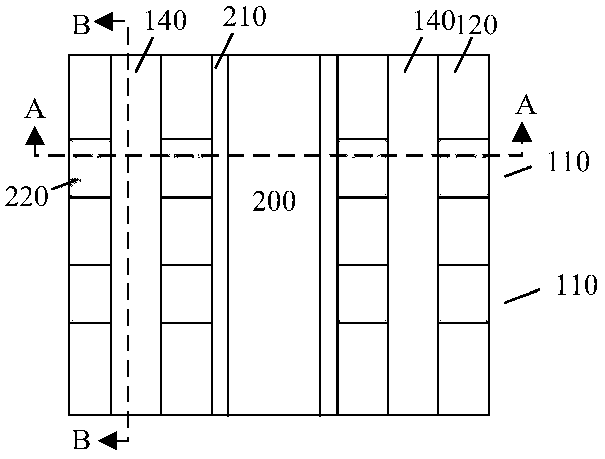
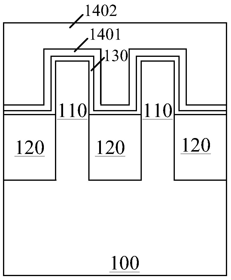
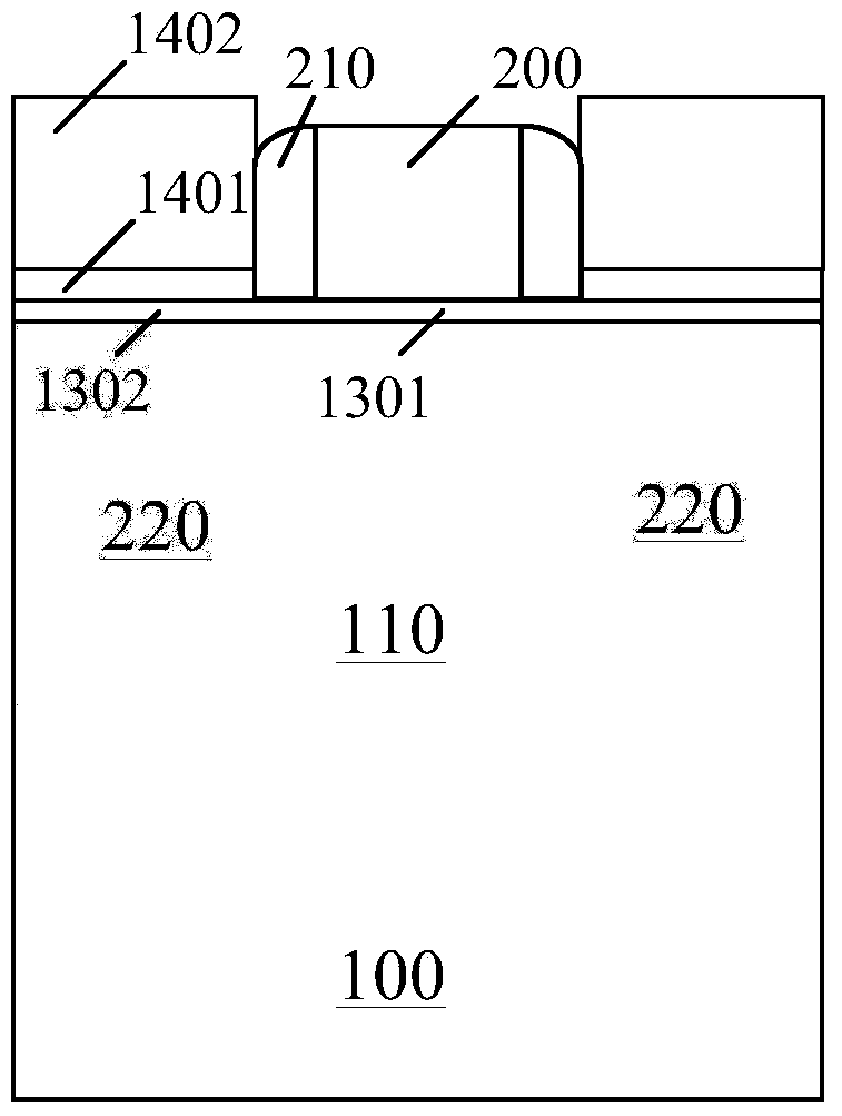
The invention provides an anti-fuse structure which comprises a semiconductor substrate, fins on the semiconductor substrate, a gate dielectric layer and gates on the surfaces of the fins, source and drain regions on the fins at the two sides of the gates, an anti-fuse medium layer on the surfaces of the source and drain regions, and upper electrodes on the anti-fuse medium layer. The anti-fuse structure based on fins has a smaller area and larger capacity, and meets the requirement for high degree of integration of devices. Moreover, the anti-fuse structure can be well compatible with fin type devices, and has good process compatibility.

Description

technical field [0001] The invention relates to the field of semiconductor devices and manufacturing, in particular to an antifuse structure and a manufacturing method thereof. Background technique [0002] An antifuse is usually a sandwich structure consisting of upper and lower electrodes and an insulating dielectric material in between. As a memory, before programming, the upper and lower electrodes of the antifuse are in a high-resistance state, usually more than a few hundred megohms, representing a storage state; during programming, a programming voltage is applied between the upper and lower electrodes, after programming, the middle The dielectric material is broken down, and the upper and lower electrodes of the antifuse are in a low resistance state, usually below a few hundred ohms, which represents another storage state. [0003] At present, the antifuse mainly adopts a planar structure, which has a relatively large area. However, with the continuous advancement ...

Claims


Application Information

Patent Timeline
Patent Type & Authority Patents(China)
IPC IPC(8): H01L23/62H01L21/02
Inventor 赵劼钟汇才
Owner INST OF MICROELECTRONICS CHINESE ACAD OF SCI
Why Eureka
Eureka Blog
Learn More