Low-power-consumption magnetic multi-resistance-state memory cell

A memory cell, multi-resistance technology, applied in the field of non-volatile memory and logic, can solve the problems of circuit design difficulty, control complexity, chip area manufacturing process and cost, etc., to improve circuit integration, facilitate optimization and design , the effect of reducing complexity and manufacturing costs

Active Publication Date: 2017-05-10
致真存储(北京)科技有限公司
View PDF4 Cites 9 Cited by
  • Summary
  • Abstract
  • Description
  • Claims
  • Application Information

AI Technical Summary

Problems solved by technology

[0009] In view of the difficulties in circuit design, control complexity, chip area, manufacturing process and cost faced by the magnetic tunnel junction writing technology mentioned in the above background, the present invention proposes a low-power magnetic multi-resistance memory unit

Method used


Image

  • Low-power-consumption magnetic multi-resistance-state memory cell
  • Low-power-consumption magnetic multi-resistance-state memory cell
  • Low-power-consumption magnetic multi-resistance-state memory cell

Examples


Embodiment Construction

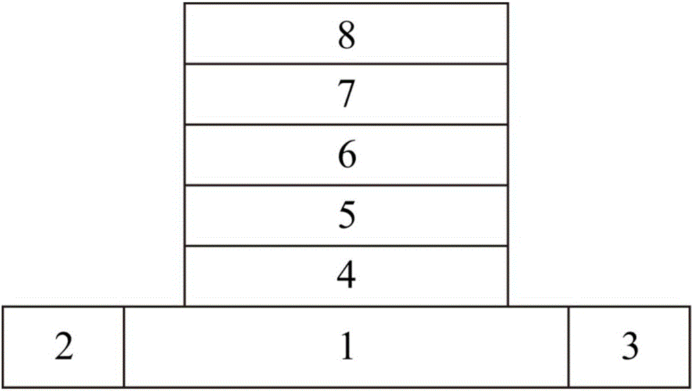
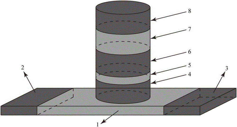
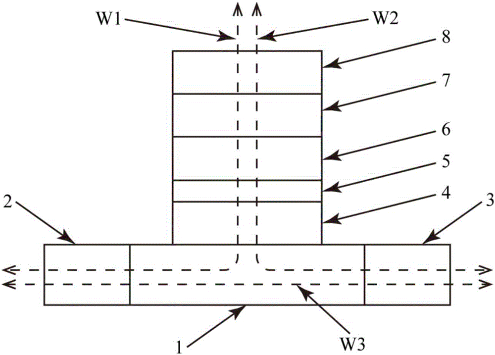
[0077] The substantive features of the present invention are further described with reference to the accompanying drawings. The drawings are all schematic diagrams, and the thicknesses of the various functional layers or regions involved are not actual dimensions, and the resistance and current values ​​in the working mode are also not actual values.

[0078] Detailed exemplary embodiments are disclosed herein, specific structural and functional details are merely representative for purposes of describing exemplary embodiments, therefore, the invention may be embodied in many alternative forms and should not be construed as It is to be construed as being limited only to the exemplary embodiments set forth herein, but to cover all changes, equivalents, and alternatives falling within the scope of the invention.

[0079] The invention provides a low-power consumption magnetic multi-resistance storage unit, which can be used not only for constructing a magnetic random access memo...


PUM


Abstract

The invention provides a low-power-consumption magnetic multi-resistance-state memory cell. The low-power-consumption magnetic multi-resistance-state memory cell successively comprises an anti-ferromagnetic strip film, a first ferromagnetic metal, a first oxide, a second ferromagnetic metal, a first synthetic anti-ferromagnetic layer and a first electrode from bottom to top. The thickness of the anti-ferromagnetic strip film is 0-20 nm. The thickness of the first ferromagnetic metal is 0-3 nm. The thickness of the first oxide is 0-2 nm. The thickness of the second ferromagnetic metal is 0-3 nm. The thickness of the first synthetic anti-ferromagnetic layer is 0-20 nm. The thickness of the first electrode is 10-200 nm. The two ends of the anti-ferromagnetic strip film are respectively plated with a second electrode and a third electrode. Five layers of materials arranged above the anti-ferromagnetic strip film form material magnetic tunnel junctions. According to the technical scheme of the invention, the multi-resistance-state storage can be realized. The low-power-consumption magnetic multi-resistance-state memory cell can be applied not only to the fields of single-bit memory and logic operation, but also the fields of brain-like calculation and the like. Data are written by adopting a unidirectional current, so that the design of memories and logic circuits is simplified. The integration level of circuits is improved and the power consumption of the memory cell is reduced. The process complexity and the manufacturing cost are reduced. Moreover, data are written by using different branches, so that the write operations of different data are independently optimized and designed.

Description

[0001] 【Technical field】 [0002] The invention relates to a low-power consumption magnetic multi-resistance storage unit, which belongs to the technical field of non-volatile storage and logic. [0003] 【Background technique】 [0004] Emerging non-volatile memory technology can keep stored data from being lost when power is turned off, so it is expected to solve the increasingly severe static problems faced by traditional memory and logic circuits based on complementary metal-oxide semiconductor (Complementary metal-oxide semiconductor, CMOS) technology. power consumption problem. Among them, Magnetic Random Access Memory (MRAM) based on Magnetic Tunnel Junction (Magnetic Tunnel Junction, MTJ) has been proved to be the The most potential general-purpose memory. It is not only expected to replace traditional SRAM (Static random access memory, SRAM) and dynamic random access memory (Dynamic random access memory, DRAM), but also can be applied to the design of non-volatile logi...

Claims


Application Information

Patent Timeline
Patent Type & Authority Applications(China)
IPC IPC(8): H01L43/10H01L43/08G11C11/56
CPCG11C11/5607G11C11/5657G11C11/5685H10N50/10H10N50/85
Inventor 赵巍胜王昭昊林晓阳粟傈张磊
Owner 致真存储(北京)科技有限公司
Why Eureka
Try Eureka