

II type superlattice photoelectric detector possessing absorption enhancement structure and manufacturing method thereof
A technology of photodetector and enhanced structure, applied in circuits, electrical components, semiconductor devices, etc., can solve the problems of high quantum efficiency, low detection accuracy, difficult to achieve, etc., to improve quantum efficiency, improve effective quality, increase overlap Effect
- Summary
- Abstract
- Description
- Claims
- Application Information
AI Technical Summary
Problems solved by technology
Method used
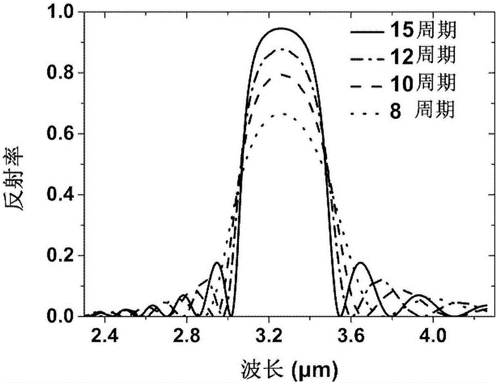
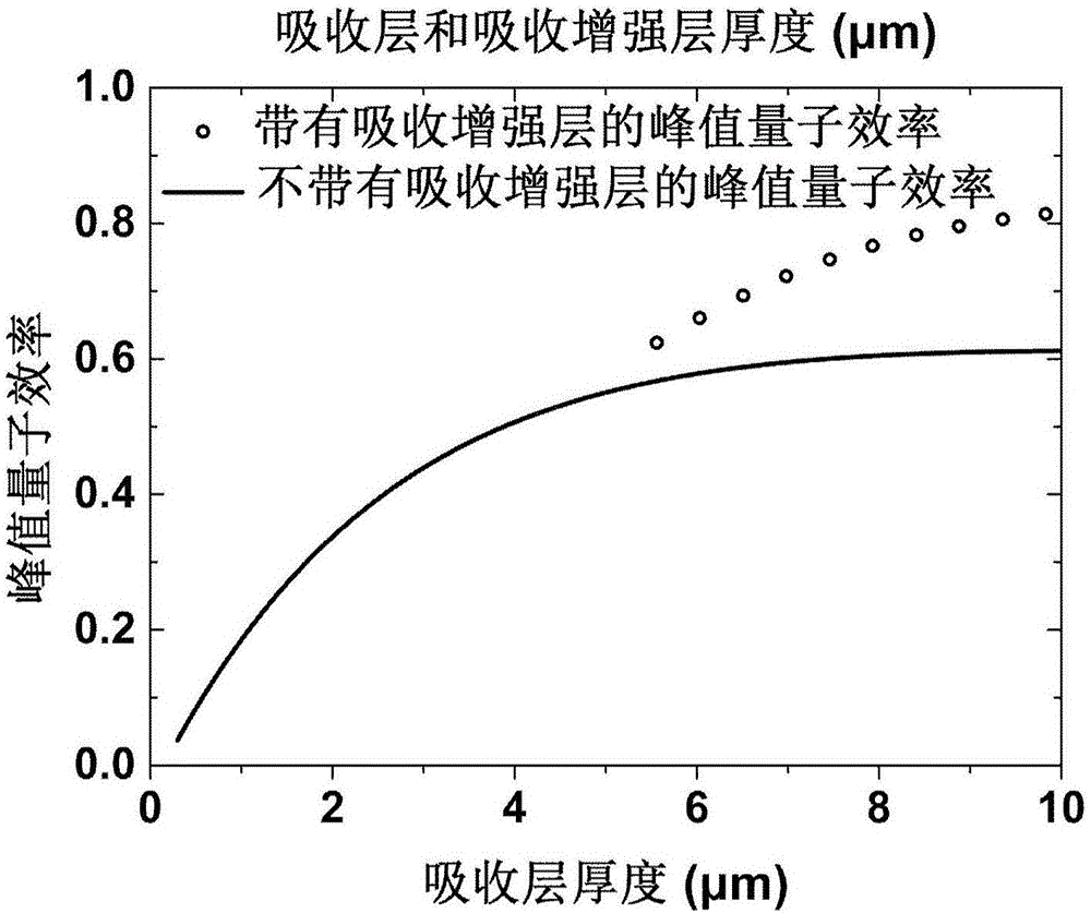
Image

Examples
preparation example Construction
[0029] One aspect of the present invention discloses a method for preparing a class II superlattice photodetector with an absorption-enhancing structure, comprising the following steps:
[0030] Step 1, forming an absorption enhancement layer on the substrate, the absorption enhancement layer is a periodic arrangement structure capable of promoting absorption enhancement;
[0031] Step 2, forming an absorbing layer on the upper surface of the absorbing enhancement layer, the absorbing layer is a type II superlattice structure;
[0032] Step 3, completing the preparation of the type II superlattice photodetector with an absorption-enhancing structure.
[0033] The absorption layer includes a p-type II superlattice layer and an n-type II superlattice layer, which are sequentially grown by molecular beam epitaxy; the p-type II superlattice layer and the n-type II superlattice layer It can be prepared by using InAs / GaSb II superlattice material, M structure II superlattice materi...
Embodiment
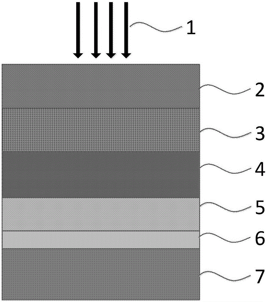
[0049] Such as figure 1 As shown, the present embodiment proposes a method for preparing a class II superlattice photodetector with an absorption-enhancing structure, comprising the following steps:
[0050] Step 1, Molecular beam epitaxial growth on the semiconductor substrate 7 to form a GaSb buffer layer 6 and an AlAs 0.09 Sb 0.91 / GaSb absorption enhancement layer 5;
[0051] Step 2, in AlAs 0.09 Sb 0.91 Molecular beam epitaxial growth on the upper surface of the GaSb absorption enhancement layer 5 forms an absorption layer, which includes a p-type II type superlattice layer 4 and an n-type II type superlattice layer 3, and the absorbed material composition It is an N structure InAs / AlSb / GaSb type II superlattice material, where each period is composed of 8ML of InAs, 2ML of AlSb and 9ML of GaSb;
[0052] Step 3, forming an InAs cap layer by epitaxial growth on the upper surface of the n-type II superlattice layer 3 in the absorbing layer, and completing the preparati...
PUM
 Abstract
Description
Claims
Application Information