Interface hermetic packaging method for electronic circuit module

An electronic circuit, hermetic packaging technology, applied in welding equipment, metal processing equipment, manufacturing tools, etc., to achieve the effect of standardized design, high efficiency, and improved efficiency

Inactive Publication Date: 2017-05-24
10TH RES INST OF CETC
View PDF6 Cites 8 Cited by
  • Summary
  • Abstract
  • Description
  • Claims
  • Application Information

AI Technical Summary

Problems solved by technology

[0005] The present invention aims at the deficiencies of the various and disordered interface designs in the past, and provides an electronic circuit component hermetic packaging interface method with reliable airtight packaging and high airtight packaging efficiency to solve the problem of high-frequency sockets commonly used in engineering, Hermetic packaging of high and low frequency electrical connectors and cylindrical head or countersunk screws

Method used


Image

  • Interface hermetic packaging method for electronic circuit module
  • Interface hermetic packaging method for electronic circuit module
  • Interface hermetic packaging method for electronic circuit module

Examples


Embodiment Construction

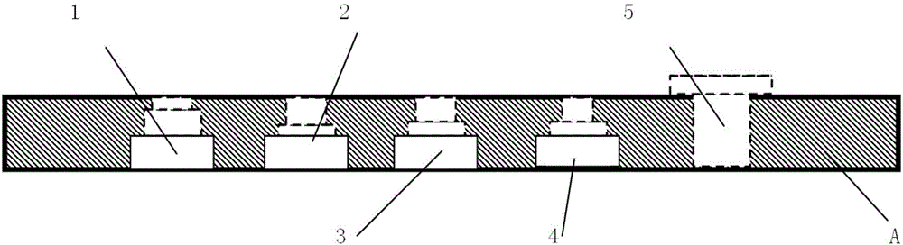
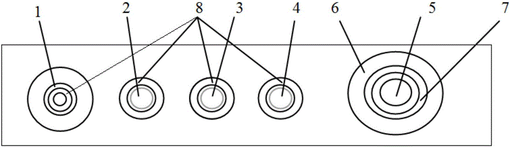
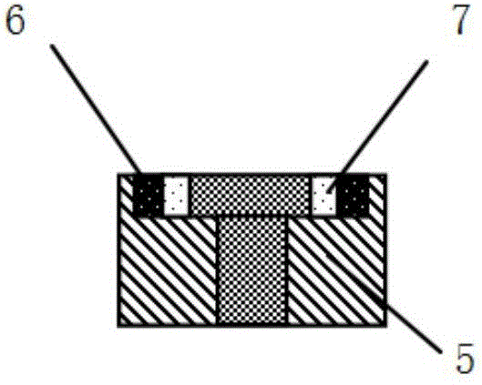
[0015] refer to Figure 1 ~ Figure 3 . According to the assembly interface of the connectors and fasteners in the electronic circuit assembly, first install the high-frequency socket 1, the first insulator 2, the second insulator 3, the third insulator 4 and the solder ring of the corresponding high-frequency socket 1; the first The solder ring of insulator 2, the solder ring of second insulator 3, and the solder ring of third insulator 4 are fixed at the positions corresponding to the preset solder ring holes 8; then the countersunk screw 5 and the shape memory alloy ring 6 are respectively assembled to their respective assembly interfaces In the vacuum welding furnace, set the welding curve that can meet the high-frequency socket 1, the first insulator 2, the second insulator 3, and the third insulator 4 at the same time, and start the welding task. When the high-frequency socket 1, the first insulator 2 After the welding of the second insulator 3 and the third insulator 4 ...


PUM


Abstract

The invention discloses an interface hermetic packaging method for an electronic circuit module. By adoption of the interface hermetic packaging method, hermetic packaging problems of high-frequency sockets, high and low frequency electric connectors and cylinder heads or sunk screws frequently used in engineering can be solved. According to the following technical scheme, the interface hermetic packaging method is achieved by comprising the steps that according to assembly interfaces of connector assemblies and fasteners in the electronic circuit module, a high-frequency socket, insulators and a soldering ring corresponding to the high-frequency socket are firstly mounted; soldering rings are fixed to corresponding preset soldering ring holes; a sunk screw and a shape memory alloy ring are separately assembled to corresponding assembly interfaces, a soldering curve meeting requirements of the devices at the same time is set in a vacuum soldering furnace, powerful contraction generated by the heated shape memory alloy ring in the soldering process squeezes a cavity and an annular wall reserved at the interface of the sunk screw, and the high-frequency socket, a radio frequency electric connector, a feed through connector and a coaxial connector in the microwave and millimeter wave electronic circuit module are integrally packaged into the cavity through the sunk screw.

Description

technical field [0001] The invention relates to an interface design method that can simultaneously meet the airtight packaging requirements of high-frequency sockets, high-low frequency electrical connectors and cylindrical head or countersunk screws in the same electronic circuit assembly. Background technique [0002] With the increasing complexity of electronic systems, there is an urgent need for high-density, high-speed and high-reliability microelectronic components or components, which must be realized by using advanced IC devices and corresponding interconnection and packaging. Throughout the electronic packaging industry in recent years, electronic packaging technology continues to develop in the direction of ultra-high density, and ultra-high-density packaging forms such as three-dimensional packaging, multi-chip packaging (MCP) and system-in-package (SIP) have emerged. Packaging technology continues to evolve towards ultra-small size. [0003] As we all know, mor...

Claims


Application Information

Patent Timeline
Patent Type & Authority Applications(China)
IPC IPC(8): B23K1/008
CPCB23K1/008
Inventor 海洋
Owner 10TH RES INST OF CETC
Why Eureka
Try Eureka