Check patentability & draft patents in minutes with Patsnap Eureka AI!

Method for preparing single crystal film

A single crystal thin film, amorphous thin film technology, applied in the field of single crystal thin film preparation, can solve problems such as crystal pollution

Inactive Publication Date: 2017-05-24
SHAANXI UNIV OF SCI & TECH
View PDF6 Cites 2 Cited by
  • Summary
  • Abstract
  • Description
  • Claims
  • Application Information

AI Technical Summary

Problems solved by technology

At present, there are various methods for preparing single crystals, including pulling method, heat exchange method and Bridgman method, etc., but these methods mostly use crucibles, which will pollute the crystals, and most of the prepared single crystals are lumpy or flaky

Method used


Image

  • Method for preparing single crystal film

Examples


preparation example Construction

[0029] A method for preparing a single crystal thin film, comprising the following steps:

[0030] First, an amorphous film is formed on the substrate 5 by means of PVD, CVD or solution coating on the substrate 5;

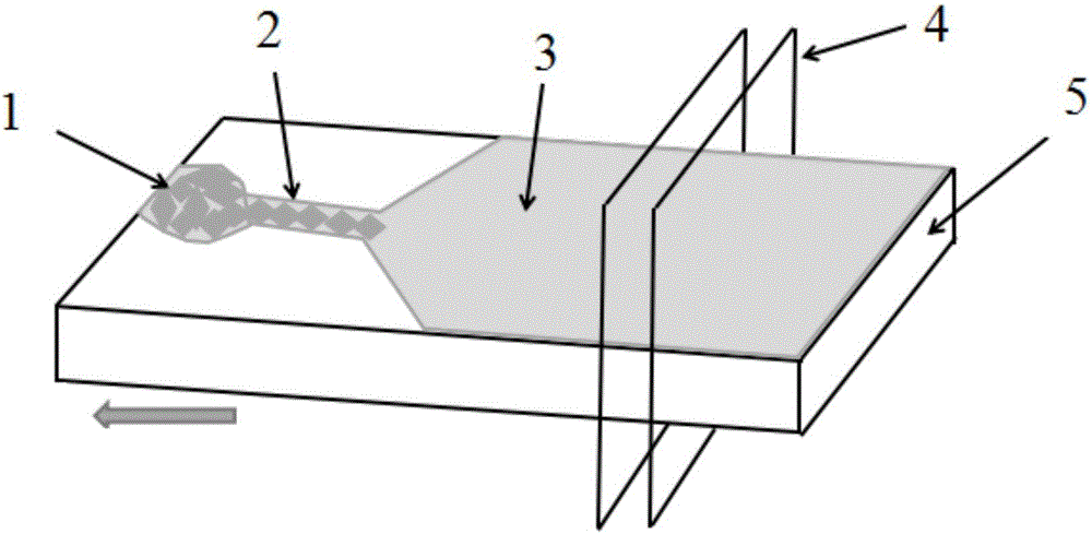
[0031] Then, the prepared amorphous film is etched to form the amorphous film figure 1 The shape shown has a region 1 for forming a polycrystalline thin film, an elongated region 2 for selectively growing a single crystal, and a region 3 for forming a single crystal thin film; the pattern can be formed by mask evaporation, or by The amorphous film is etched by solution etching method or plasma etching method, thus forming such as figure 1 The interconnected three-segment structure shown: the second region 2 is an elongated structure whose width is smaller than the minimum width for polycrystalline formation;

[0032] Finally, by means of heat treatment, laser irradiation, microwave treatment or electromagnetic radiation heating, each region of the amorphous film ...

Embodiment

[0037] First, an a-Si thin film is formed on the substrate 5 by PVD;

[0038] Then, photolithography is performed on the prepared a-Si thin film to form the figure 1 The shape shown has an interconnected three-section structure: a region 1 for forming a polycrystalline Si film, a region 2 for selectively growing a single crystal, and a region 3 for forming a single crystal Si film, wherein the second region 2 is a thin Long structures, the width of which is not more than 1cm;

[0039] Finally, by means of heat treatment, laser irradiation, microwave treatment or electromagnetic radiation heating, each region of the a-Si thin film is sequentially processed to make it gradually crystallize, and a polycrystalline Si region, a selective region and a single crystal Si film region are sequentially formed on the substrate. , and finally remove the polycrystalline Si region and the selective region to obtain a single crystal Si film.

[0040] In addition, the amorphous thin film of ...


PUM


Abstract

The invention discloses a method for preparing a single crystal film and relates to the technical field of single crystal film preparation, in particular to a method for performing heat treatment on an amorphous film with a specific shape to prepare the single crystal film. First the amorphous film is formed on a substrate; the film is processed to form a three-section shape; each area of the amorphous film is processed sequentially through means of heat treatment, laser radiation and microwave processing or electromagnetic radiation heating and the like, so that the amorphous film is gradually crystallized, a polycrystalline area, a selection area and a single crystal film area are sequentially formed on a substrate, and finally the polycrystalline area and the selection area are removed to obtain the single crystal film.

Description

[0001] 【Technical field】 [0002] The invention relates to the technical field of single crystal thin film preparation, in particular to a preparation method of single crystal thin film. [0003] 【Background technique】 [0004] Single crystals are continuous throughout their lattice and have important industrial applications. At present, there are various methods for preparing single crystals, including pulling method, heat exchange method and Bridgman method, etc., but these methods mostly use crucibles, which will pollute the crystals, and most of the prepared single crystals are Lumpy or flaky. [0005] At the same time, in order to obtain an ideal single crystal, it is usually necessary to add a single crystal seed crystal as the starting point of crystal growth. On the one hand, the seed crystal is used as a replica sample, so that the prepared single crystal and the seed crystal have the same crystal orientation; on the other hand, the seed crystal The crystal is used a...

Claims


Application Information

Patent Timeline
IPC IPC(8): C30B29/64C30B1/02
CPCC30B1/02C30B29/64
Inventor 张方辉聂屈洋孙立蓉牟强王江南张婵婵李亭亭刘晋红
Owner SHAANXI UNIV OF SCI & TECH
Features
  • R&D
  • Intellectual Property
  • Life Sciences
  • Materials
  • Tech Scout
  • Unparalleled Data Quality
  • Higher Quality Content
  • 60% Fewer Hallucinations
Learn More