Control swap gate optical logic device based on micro-ring resonators

A micro-ring resonator and optical logic technology, applied in the field of optical logic computing, can solve the problems that low-power device design cannot be ignored, limit chip performance and computing speed, bit loss, etc., achieve high-speed large-capacity information processing, power Low consumption and fast speed

Active Publication Date: 2017-05-24
LANZHOU UNIVERSITY
View PDF3 Cites 8 Cited by
  • Summary
  • Abstract
  • Description
  • Claims
  • Application Information

AI Technical Summary

Problems solved by technology

[0004] Computer operations are all binary number calculations, and the existing traditional non-reversible logic devices are mainly non-reversible logic gates with two inputs and one output. When the input information passes through the gate, one output information bit will be lost. As early as 1960, R.Landauer proposed It has been proved that every operation of irreversible computing will cause the loss of bits, and every time a bit of information is lost, kTln2 heat energy will be dissipated. Although the energy loss is very small at room temperature, it cannot be ignored for the design of low-power devices
At the same time, the heat generated by energy consumption will greatly limit the performance and computing speed of the chip

Method used


Image

  • Control swap gate optical logic device based on micro-ring resonators
  • Control swap gate optical logic device based on micro-ring resonators
  • Control swap gate optical logic device based on micro-ring resonators

Examples


Embodiment Construction

[0028] The present invention will be further described below in conjunction with the accompanying drawings and specific embodiments.

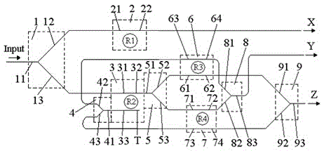
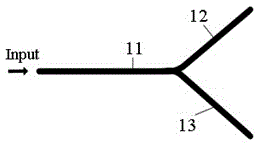
[0029] Such as figure 1 As shown, the optical logic device of the present invention includes a structure such as figure 2 The first Y-branch coupler 1 shown, the first Y-branch coupler 1 is composed of a first input optical waveguide 11, a first straight-through optical waveguide 12 and a second straight-through optical waveguide 13, one end of the first input optical waveguide 11 Connecting to the optical signal input, the other end of the first input optical waveguide 11 is respectively connected to one end of the first straight-through optical waveguide 12 and one end of the second straight-through optical waveguide 13;

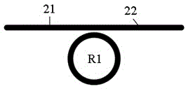
[0030] structured as image 3 The first shown microring resonator 2, the first microring resonator 2 is made up of the first silicon-based nanowire microring R1 and the first straight waveguide, the first straight wavegu...


PUM

PropertyMeasurementUnit
refractive indexaaaaaaaaaa

Abstract

The invention provides a control swap gate optical logic device based on micro-ring resonators. The control swap gate optical logic device is characterized in that the control swap gate optical logic device is composed of four micro-ring resonators MRR made of a semiconductor material on an insulator and five Y-branch couplers, wherein three inputs are electrical signals to be operated and one continuous optical signal located at an operating wavelength position, an output result is an optical signal obtained after control swap gate calculation is conducted on the electrical signals, the optical signal can be transmitted in an optical fiber and directedly undergoes next-stage optical information processing. The control swap gate optical logic device is provided with the three electric pulse sequence inputs to be calculated, and an output is an optical pulse sequence obtained after calculation. A control swap gate optical logic device manufacturing process is completely compatible with a COMS process, so that the device is small in size, high in speed, low in power consumption and convenient to integrate and is hopeful to play the important role in a photon computer.

Description

technical field [0001] The invention belongs to the field of optical logic computing, and relates to a control switching gate optical logic device based on a microring resonator, which is suitable for the fields of optical communication and optical computing. Background technique [0002] Existing computers transmit and process information electronically. With the advancement of semiconductor process technology, the size of transistors is getting smaller and smaller, and the number of transistors that can be integrated on a chip is increasing. When the CPU obtains a higher main frequency, the power consumption rises sharply, and the leakage and heat dissipation problems cannot be solved. . From the perspective of the development of high-speed computers, the use of electrons as transport information carriers can no longer meet people's requirements for faster processing speeds of computers, which shows that the ability to improve the computing speed of existing computers is ...

Claims


Application Information

Patent Timeline
Patent Type & Authority Applications(China)
IPC IPC(8): G02F3/00
Inventor 田永辉刘子龙李德钊赵永鹏赵国林肖恢芙杨建红吴小所
Owner LANZHOU UNIVERSITY
Why Eureka
Try Eureka