Exposure device and method

一种曝光装置、曝光方法的技术,应用在照相制版工艺曝光装置、微光刻曝光设备、光学等方向,能够解决难以满足大批量的生产需求、无法用LED光刻领域、机器良率低等问题,达到改善侧壁陡度、降低敏感度、提高良率的效果

Active Publication Date: 2017-05-24
SHANGHAI MICRO ELECTRONICS EQUIP (GRP) CO LTD
View PDF4 Cites 0 Cited by
  • Summary
  • Abstract
  • Description
  • Claims
  • Application Information

AI Technical Summary

Problems solved by technology

Please refer to figure 2 , the mask 20 in the prior art adopts a quadrangular shape, and the mask can be spliced ​​into a square. The lighting system and mask of this structure are mainly used in the field of laser annealing, and cannot be used in the field of LED lithography.
[0005] At present, lithography machines for exposing patterned sapphire substrate patterns are affected by factors such as lens design cost or control system design. These machines have low yield and poor adaptability, and it is difficult to meet the needs of mass production.

Method used


Image

  • Exposure device and method
  • Exposure device and method
  • Exposure device and method

Examples


Embodiment 1

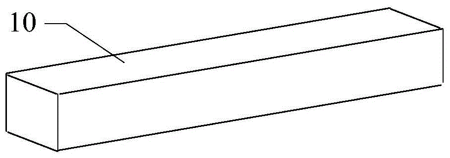
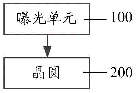
[0046] Please refer to Figures 3 to 6 , this embodiment provides an exposure device, including an exposure unit 100 for exposing a wafer 200; the exposure unit 100 includes an illumination system 110 and a mask 120, the illumination system 110 includes a uniform light unit 113, so The uniform light unit 113 includes a regular hexagonal uniform light quartz rod 1131 , and the shape of the mask 120 is a regular hexagon matching the uniform light quartz rod 1131 .

[0047] Please refer to Figures 5 to 8 In the exposure device of the present invention, the uniform light quartz rod 1131 of the uniform light unit 113 in the illumination system 110 is improved from a quadrangle to a regular hexagon, and the mask 120 is matched and designed to be a regular hexagon. Figure 7 -8 is the effect diagram of the relationship between the objective field of view and the exposure field of view, please refer to Figure 8 , in the case of the same exposure field of view, the diagonal length ...

Embodiment 2

[0057] The second embodiment provides an exposure method. The second embodiment is based on the exposure device of the first embodiment, and includes at least the following steps: designing a light-diffusing quartz rod in a light-diffuser unit of an illumination system into a regular hexagon shape, The shape of the mold is designed to match the regular hexagonal step of the dodging quartz rod for exposure. Under the same exposure field of view, the diagonal length of the regular hexagonal exposure field of view reflected by the regular hexagonal uniform light quartz rod is shorter than the diagonal length of the quadrilateral exposure field of view, thus reducing the projection objective. The focal depth of the projection objective improves the actual useful focal depth of the projection objective; under the same focal depth of the projection objective, the regular hexagonal exposure field of view reflected by the regular hexagonal uniform light quartz rod is greater than the e...


PUM


Abstract

The invention discloses an exposure device. The exposure device comprises an exposure unit used for preforming exposure on a wafer, wherein the exposure unit comprises an illuminating system and masks, and the illuminating system comprises a dodging unit. The exposure device is characterized in that the dodging unit comprises orthohexagonal dodging quartz rods; and each mask is in an orthohexagonal shape matched with that of each orthohexagonal dodging quartz rod. Through the adoption of the exposure device disclosed by the invention, under the situation of the same exposure field of view, the influence of field curvature of an objective lens on depth of focus is reduced, and the depth of focus, which can be used in practice, is increased; and under the situation of the same depth of focus of projection objective lenses, the exposure area of the exposure field of view is expanded.

Description

technical field [0001] The present invention relates to a lithography apparatus, in particular to an exposure device and method. Background technique [0002] A lithographic apparatus is a machine that applies a desired pattern to a substrate, usually a target portion of the substrate. For example, lithographic apparatuses can be used in the manufacture of integrated circuits. In this case, a patterning device, which may be considered a mask or reticle, is used to generate a circuit pattern corresponding to a single layer of the integrated circuit. The pattern can be imaged onto a target portion (eg, including a portion of a die, one or more dies) on a substrate (eg, a silicon wafer). In particular, in the field of LED manufacturing, it is first necessary to image the dense hole pattern onto the patterned sapphire substrate. [0003] Compared with the imaging of lines, the imaging of dense holes or dense cylinders will be much more difficult, and the actual depth of focus...

Claims


Application Information

Patent Timeline
Patent Type & Authority Applications(China)
IPC IPC(8): G03F7/20G02B27/09
CPCG02B27/09H01L33/00G03F7/2022G03F7/20G03F7/70641G03F7/70775G03F7/70833H01L21/673H01L21/67763H01L21/682G03F7/70075G03F7/2008H01L21/027H01L21/67069
Inventor 谢仁飚杨志勇白昂力王健
Owner SHANGHAI MICRO ELECTRONICS EQUIP (GRP) CO LTD
Why Eureka
Try Eureka