A debugging structure for GPU unified coloring processing array

An array and unified technology, applied in the debugging structure field of GPU uniform dyeing processing array, can solve problems such as poor portability, inability to guarantee circuit, safety, reliability, security risks, etc., and achieve the goal of reducing difficulty and reducing the range of storage space Effect

Active Publication Date: 2020-04-07
XIAN AVIATION COMPUTING TECH RES INST OF AVIATION IND CORP OF CHINA
View PDF5 Cites 0 Cited by
  • Summary
  • Abstract
  • Description
  • Claims
  • Application Information

AI Technical Summary

Problems solved by technology

[0003] At present, there is no GPU based on a unified dyeing architecture in my country, and a large number of commercial GPU chips imported from abroad are used in display control systems in various fields.
Especially in the military field, foreign imported commercial GPU chips have poor temperature and environmental adaptability, cannot guarantee that the circuit itself or supporting software has no "back door", contains a large number of redundant functional units that are not needed in the military field, and the power consumption index cannot meet the requirements. Commercial GPU chips are updated quickly, facing production stoppages and outages at any time, making it difficult to meet defects such as continuous support of weapons and equipment, and there are major hidden dangers in terms of safety, reliability, and support.
Moreover, due to political, military, economic and other reasons, foreign countries have implemented technology "blockade" and product "monopoly" on my country, making it difficult to obtain the underlying technical information of GPU chips, such as register information, detailed internal micro-architecture, core software source code, etc., resulting in GPU functions and performance cannot be fully utilized, and the portability is poor; the above problems seriously restrict the independent research and development of display systems in my country

Method used


Image

  • A debugging structure for GPU unified coloring processing array

Examples


Embodiment

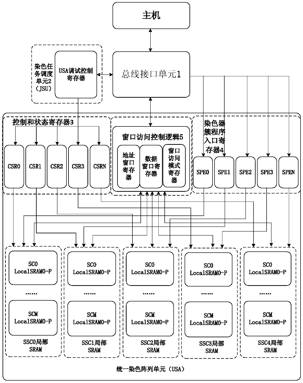
[0051] Such as figure 1 As shown, the host can configure the window access mode register in the window control logic through the register channel in the PCIe module, so as to choose to work in the normal working mode or the debugging working mode.

[0052] In the debugging working mode, there may be differences in the access procedures of different implementation solutions, but this does not make the essence of the corresponding implementation solutions deviate from the spirit and scope of the solutions of the present invention. The typical process of host debugging access to the unified dyeing array is as follows:

[0053] In the first step, the host sequentially accesses the address and data window registers in the window control logic through the register channel of the bus interface unit, writes the local memory address and write flag of the shader cluster to be written, and the data to be written. The window control logic will write any specified dyeing task attribute da...


PUM


Abstract

The invention provides a debugging structure for a GPU unified dyeing processing array. The debugging structure comprises a bus interface unit between a GPU and a host, a dyeing task scheduling unit, a control and status register in a plurality of unified dyeing arrays, a plurality of dyestuff cluster program entry registers, and window access control logic which accesses a local memory in the unified dyeing arrays. According to the invention, based on the functional units, any number of dyeing tasks can be continuously injected into the unified dyeing arrays, wherein the number of dyeing tasks does not exceed the maximum number of tasks; the type of each dyeing task can be arbitrarily specified; the processing method of different kinds of dyeing tasks can be arbitrarily specified; and the host can acquire the processing result of all dyeing tasks.

Description

technical field [0001] The invention relates to the technical field of computer hardware, in particular to a debugging structure of a GPU unified dyeing processing array. Background technique [0002] With the continuous increase of graphics applications, the early solution of graphics rendering by CPU alone has been difficult to meet the graphics processing needs of performance and technology growth, and the graphics processing unit (Graphic Processing Unit, GPU) came into being. Since the release of the first GPU product by Nvidia in 1999, the development of GPU technology has mainly gone through the fixed-function pipeline stage, the stage of separating the dyer architecture, and the stage of unified dyer architecture. Rendering gradually extends to the field of general computing. The high-speed, parallel features and flexible programmability of the GPU pipeline provide a good operating platform for graphics processing and general parallel computing. [0003] At present...

Claims


Application Information

Patent Timeline
Patent Type & Authority Patents(China)
IPC IPC(8): G06T1/20G06F9/50
CPCG06F9/5044G06T1/20
Inventor 张骏田泽任向隆韩立敏郑新建牛少平
Owner XIAN AVIATION COMPUTING TECH RES INST OF AVIATION IND CORP OF CHINA
Why Eureka
Try Eureka