

Photolithography solution prediction method based on layout geometric feature matching
A solution and geometric feature technology, applied in the field of lithography solution prediction based on layout geometric feature matching, can solve problems such as inability to intuitively feedback layout design, inability to analyze unknown or undetected, and inability to provide unknown layout graphics, etc. Achieve the effect of shortening the development cycle, ensuring successful implementation, and reducing selection time
- Summary
- Abstract
- Description
- Claims
- Application Information
AI Technical Summary
Problems solved by technology
Method used
Image

Examples
Embodiment 1
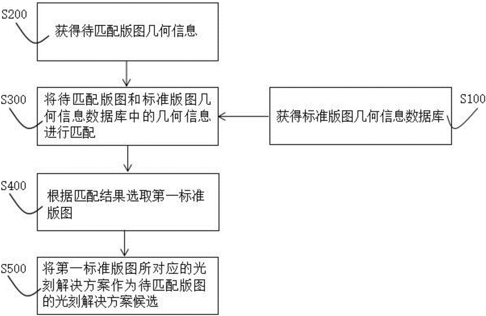
[0035] Embodiment 1 provides a lithography solution prediction method based on layout geometric feature matching, such as figure 1 As shown, the method includes:
[0036] S100: Obtain a standard layout geometric information database;
[0037] S200: Obtain geometric information of the layout to be matched;
[0038] S300: Match the layout geometric information to be matched with the geometric information in the standard layout geometric information database;
[0039] S400: Select a first standard layout according to the matching result;
[0040] S500: Using the lithography solution corresponding to the first standard layout as a candidate for the lithography solution of the layout to be matched, and predicting the lithography solution of the layout to be matched.
[0041] Embodiment 1 By establishing a standard layout geometric information database, the geometric information of the layout to be matched is obtained, and the statistical results of the geometric information of t...
Embodiment 2
[0045] Embodiment 2 provides a lithography solution prediction method based on layout geometric feature matching, the method comprising:
[0046] Obtain a standard layout geometric information database;
[0047] Obtain geometric information of the layout to be matched;
[0048] matching the layout geometric information to be matched with the geometric information in the standard layout geometric information database;
[0049] selecting a first standard layout according to the matching result;
[0050] The lithography solution corresponding to the first standard layout is used as a candidate lithography solution of the layout to be matched, and the lithography solution of the layout to be matched is predicted.
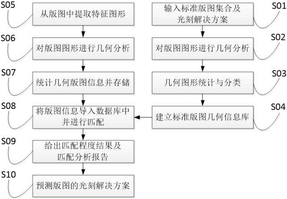
[0051] Wherein, said obtaining standard layout geometric information database includes:
[0052] Obtain the standard layout collection and the lithography solution corresponding to each standard layout in the collection;
[0053] Obtaining geometric information of t...
PUM
 Abstract
Description
Claims
Application Information