Optimization method designed with integrated circuit mask design and storage medium accessible to computer

A mask design and integrated circuit technology, applied in the field of optimization methods and computer-readable storage media, can solve the problems of long mask optimization time and high optimization cost, achieve fast mask optimization, accelerate optimization speed, and reduce design defects graphic effects

Active Publication Date: 2017-05-31
DONGFANG JINGYUAN ELECTRON LTD
View PDF5 Cites 26 Cited by
  • Summary
  • Abstract
  • Description
  • Claims
  • Application Information

AI Technical Summary

Problems solved by technology

[0008] In order to overcome the problems of long optimization time and high optimization cost of the full-chip inversion lithography mask ...

Method used


Image

  • Optimization method designed with integrated circuit mask design and storage medium accessible to computer
  • Optimization method designed with integrated circuit mask design and storage medium accessible to computer
  • Optimization method designed with integrated circuit mask design and storage medium accessible to computer

Examples


Embodiment Construction

[0041] In order to make the purpose, technical solutions and advantages of the present invention more clear, the present invention will be further described in detail below in conjunction with the accompanying drawings and implementation examples. It should be understood that the specific embodiments described here are only used to explain the present invention, not to limit the present invention.

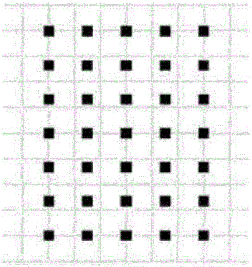
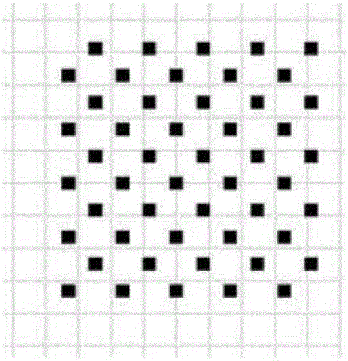
[0042] see figure 1 , The invention provides an optimization method for mask design of an integrated circuit. This embodiment is an example of the layout design of the via layer (VIA) of the 14nm node logic circuit, which can be divided into the following steps S1-S6:

[0043] Step S1: Provide a full-chip design layout of an integrated circuit, and randomly capture multiple small areas of the design layout in the full-chip design layout.

[0044] Specifically, the current large-scale integrated circuits are generally manufactured using a photolithography system. The lithography ...


PUM


Abstract

The invention provides an optimization method with integrated circuit mask design. The optimization method comprises the steps of S1, providing a whole chip design layout of an integrated circuit, and randomly grasping multiple design layout small areas in the whole chip design layout; S2, conducting mask optimization which is based on pixels on the chosen design layout small areas, and outputting a pixel grey-scale map of mask layout of each design layout small area; S3, utilizing the design layout small area mask pixel grey-scale maps obtained in the step S2 and small area design layouts corresponding to the design layout small area mask pixel grey-scale maps, and establishing a BP artificial neural network model; S4, sending the whole chip design layout into the BP artificial neural network model established in the step S3 to obtain a mask design layout grey-scale map of the whole chip design layout. The invention further provides a medium of a computer program used for storing the integrated circuit mask design.

Description

[0001] 【Technical field】 [0002] The invention relates to the field of mask manufacturing of integrated circuits, in particular to an optimization method for mask design of integrated circuits and a computer-readable storage medium. [0003] 【Background technique】 [0004] The photolithography process is the most important manufacturing process in the modern ultra-large-scale integrated circuit manufacturing process, that is, an important means to transfer the design pattern of the integrated circuit on the mask to the silicon wafer through the photolithography machine. When the integrated circuit design pattern on the mask is imaged on the silicon wafer through the projection objective lens of the lithography machine, as the feature size of the pattern on the mask becomes smaller, the diffraction phenomenon of light becomes more and more significant. [0005] After undergoing rule-based optical proximity correction and model-based optical proximity correction, the most advanc...

Claims


Application Information

Patent Timeline
IPC IPC(8): G06F17/50
CPCG06F30/39G03F1/36G06N3/04
Inventor 张生睿俞宗强施伟杰
Owner DONGFANG JINGYUAN ELECTRON LTD
Why Eureka
Try Eureka