Crystallization method of metal oxide semiconductor layer, semiconductor structure, active array substrate, and indium gallium zinc oxide crystal

A technology of oxide semiconductor and oxide layer, which is applied in semiconductor devices, semiconductor/solid-state device manufacturing, transistors, etc., and can solve the problems of thin film transistor yield decline and active layer damage

Active Publication Date: 2017-05-31
AU OPTRONICS CORP
View PDF6 Cites 11 Cited by
  • Summary
  • Abstract
  • Description
  • Claims
  • Application Information

AI Technical Summary

Problems solved by technology

However, when the etchant removes the metal layer above the active layer, the active layer is easily damaged due to exposure to the etchant, resulting in a decrease in the yield of the thin film transistor.

Method used


Image

  • Crystallization method of metal oxide semiconductor layer, semiconductor structure, active array substrate, and indium gallium zinc oxide crystal
  • Crystallization method of metal oxide semiconductor layer, semiconductor structure, active array substrate, and indium gallium zinc oxide crystal
  • Crystallization method of metal oxide semiconductor layer, semiconductor structure, active array substrate, and indium gallium zinc oxide crystal

Examples


Embodiment Construction

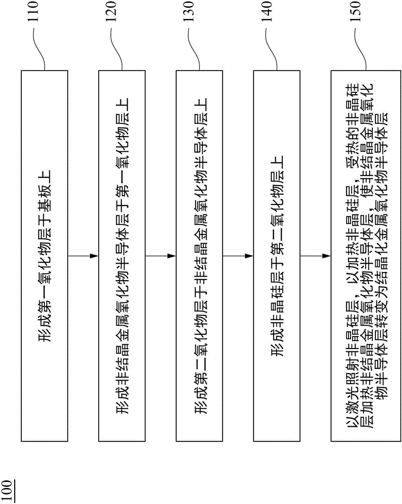
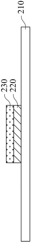
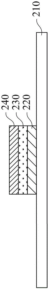
[0109] The objects and advantages of the present invention will be more apparent through the detailed description of the accompanying drawings and reference symbols in the following embodiments.

[0110] In order to make the description of the present disclosure more detailed and complete, reference may be made to the attached drawings and the various embodiments described below. The same numbers in the drawings represent the same or similar elements, and for clarity, the size of the elements Or the thickness may be exaggerated and not drawn according to the original size. In addition, for the sake of simplifying the drawings, some structures and elements will be shown in a simple schematic way in the drawings. However, it should be understood that the provided embodiments are not intended to limit the scope of the present invention. These practical details should not be used to limit the invention. That is, in some embodiments of the present invention, these practical detai...


PUM

PropertyMeasurementUnit
sizeaaaaaaaaaa
thicknessaaaaaaaaaa

Abstract

The present invention provides a method for crystallizing a metal oxide semiconductor layer, a semiconductor structure, a method for fabricating the semiconductor structure, an active array substrate, and an indium gallium zinc oxide crystal. The crystallization method comprises the steps of: forming an amorphous metal oxide semiconductor layer over a substrate; forming an oxide layer on the non-crystalline metal oxide semiconductor layer; forming an amorphous silicon layer on the oxide layer; irradiating an amorphous silicon layer with a laser to heat the amorphous silicon layer and heating the amorphous metal oxide semiconductor layer with the heated amorphous silicon layer to convert the non-crystalline metal oxide semiconductor layer into a crystalline metal oxide semiconductor layer.

Description

technical field [0001] The present invention relates to the crystallization method of the metal oxide semiconductor layer, the semiconductor structure, the manufacturing method of the semiconductor structure, the active array substrate, and the indium gallium zinc oxide crystal, especially about the use of the heated amorphous silicon layer as a heat source to crystallize the amorphous metal A method for an oxide semiconductor layer, and a semiconductor structure and an active array substrate formed by the method. Background technique [0002] In recent years, due to the advancement of semiconductor manufacturing technology, the process of thin-film transistors (Thin-film transistors, TFTs) has also become simpler and faster, making TFTs widely used in computer chips, mobile phone chips, TFT liquid crystal displays (Liquid crystal display, LCD )Wait. Among them, a commonly used method for fabricating thin film transistors is back channel etch (Back channel etch, BCE), which...

Claims


Application Information

Patent Timeline
Patent Type & Authority Applications(China)
IPC IPC(8): H01L21/336H01L29/786H01L27/12
CPCH01L27/1214H01L29/66742H01L29/7869H01L27/1225H01L27/124H01L27/1251H01L27/1274H01L29/66969H01L29/78675H01L21/02565H01L21/02672H01L27/1218H01L29/045
Inventor 叶家宏黄景亮
Owner AU OPTRONICS CORP
Why Eureka
Try Eureka