Flexible display panel and manufacturing method thereof

A flexible display and flexible substrate technology, applied in semiconductor/solid-state device manufacturing, electrical components, electrical solid-state devices, etc., can solve the limitation of the application scope and bending method of flexible OLED screens, partial peeling of OLED light-emitting layers, and uneven screen stress. problem, to avoid local peeling, improve packaging effect, and improve bending resistance.

Inactive Publication Date: 2017-05-31
WUHAN CHINA STAR OPTOELECTRONICS TECH CO LTD
View PDF18 Cites 41 Cited by
  • Summary
  • Abstract
  • Description
  • Claims
  • Application Information

AI Technical Summary

Problems solved by technology

Although the inorganic layer in TFE has strong adhesion to the array layer on the substrate, the contact area is relatively small
When the flexible OLED screen is impacted by external force, or in the process of multiple bending/curling, the i...

Method used


Image

  • Flexible display panel and manufacturing method thereof
  • Flexible display panel and manufacturing method thereof
  • Flexible display panel and manufacturing method thereof

Examples


Embodiment 1

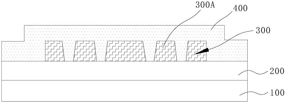
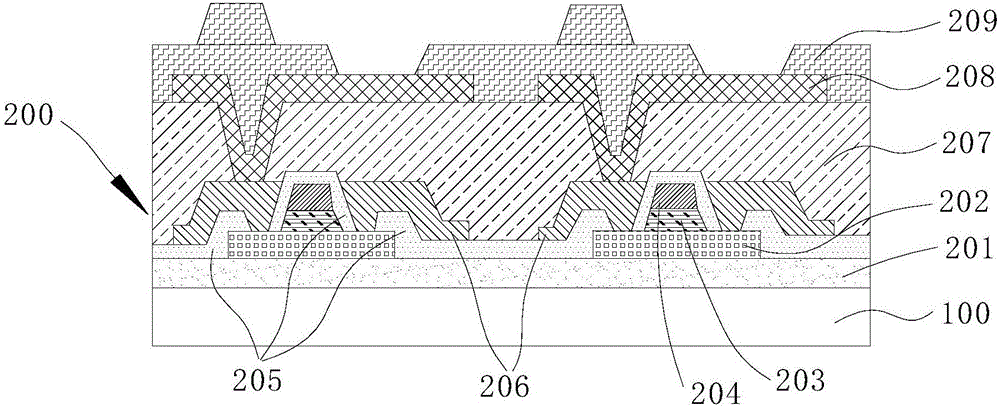
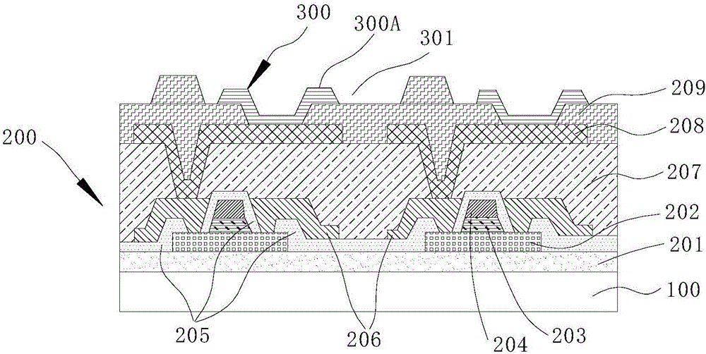
[0034] refer to figure 1 , the flexible display panel of this embodiment includes a flexible substrate layer 100, an array substrate layer 200, an organic light-emitting layer 300, and a thin-film encapsulation layer 400 stacked vertically in sequence, wherein the effective display area of ​​the organic light-emitting layer 300 includes a light-emitting area with sub-pixels 300A and the non-light-emitting area (not shown) next to the light-emitting area 300A, that is, the area between two adjacent light-emitting areas 300A is the non-light-emitting area. combine image 3 As shown, the non-light-emitting area is provided with a recessed portion 301 with a hole structure, and the thin film encapsulation layer 400 is deposited on the surface of the organic light-emitting layer 300 and in the recessed portion 301 .

[0035] Preferably, the thin film encapsulation layer 400 is alternately deposited on the surface of the flexible OLED layer 300 using polymer organic films and inorg...

Embodiment 2

[0046] like Figure 7 As shown, as another implementation manner, the recessed portion 301 further extends through the pixel defining layer 209 to the anode layer 208 , and the thin film encapsulation layer 400 is deposited on the surface of the anode layer 208 or the planar layer 207 .

[0047] The difference from the fabrication method in Example 1 is that specifically in the fabrication step (2) of the flexible display panel, it is necessary to further etch the array substrate layer 200 when fabricating the recessed portion 301 so that the recessed portion 301 further penetrates the pixel defining layer 209 , and then, the thin film encapsulation layer 400 may be deposited on the surface of the anode layer 208 or the planar layer 207 .

Embodiment 3

[0049] like Figure 8 As shown, as yet another embodiment, the depth of the recessed portion 301 is further extended relative to the embodiment 1, sequentially passing through the pixel defining layer 209, the anode layer 208, the planar layer 207 to the interlayer insulating layer 205, and the thin film encapsulation layer 400 is deposited on the surface of the interlayer insulating layer 205 .

[0050] The difference from the fabrication method in Example 1 is that, specifically in the fabrication step (2) of the flexible display panel, it is necessary to further etch the array substrate layer 200 when fabricating the recessed portion 301 so that the recessed portion 301 further penetrates the pixel defining layer 209 , the anode layer 208 , the flat layer 207 to the interlayer insulating layer 205 , and then, the thin film encapsulation layer 400 may be deposited on the surface of the interlayer insulating layer 205 .


PUM


Abstract

The invention discloses a flexible display panel. The flexible display panel comprises a flexible substrate layer, an array substrate layer, an organic light emitting diode layer and a thin film encapsulation layer which are sequentially overlapped in the longitudinal direction. The effective display area of the organic light emitting diode layer comprises a luminous area with sub-pixels and a non-luminous area beside the luminous area, wherein the non-luminous area is provided with a recess unit, and the thin film encapsulation layer is deposited on the surface of the organic light emitting diode layer and inside the recess unit. The invention also discloses a manufacturing method of the flexible display panel. By increasing the contact area and the contact positions between the TFE (thin film encapsulation) layer and the Array layer, the flexible display panel can effectively enhance the bonding force between the TFE layer and the Array layer, avoids local peeling of the OLED (organic light emitting diode) layer of a screen under external force and further improve the impact resisting and bending resisting performance of the screen. Besides, the applied encapsulation manner of the flexible display panel can effectively release the internal stress of the TFE layer to further improve the bending resisting performance of the screen; meanwhile, the TFE structure prolongs the path length of water permeation and further enhances the encapsulation effects.

Description

technical field [0001] The present invention relates to a flexible display device, in particular to a flexible display panel and a manufacturing method thereof. Background technique [0002] With the development of display technology, although TFT-LCD (thin film transistor-liquid crystal display, thin film transistor liquid crystal display) technology still occupies the mainstream display market, centered on OLED (Organic Light-Emitting Diode, organic light-emitting diode), the new The development and application of the first-generation display technology is in full swing and has been gradually applied to many fields: wearable devices such as smart bracelets, smart watches, VR (Virtual Reality, virtual reality) equipment, mobile phones, e-books and e-newspapers , TV sets, personal portable computers, etc. [0003] Compared with traditional TFT-LCD technology, the biggest advantage of OLED is that it can be made into foldable / rollable products. In order to achieve the flexi...

Claims


Application Information

Patent Timeline
IPC IPC(8): H01L27/12H01L21/77
Inventor 崔磊
Owner WUHAN CHINA STAR OPTOELECTRONICS TECH CO LTD
Why Eureka
Try Eureka