A Schottky diode
A technology of Schottky diodes and anodes, which is applied in semiconductor devices, electrical components, circuits, etc., can solve the problems of low reverse leakage current and large reverse bias, so as to reduce reverse leakage current and positive current The effect of leading conduction voltage drop and increasing reverse withstand voltage capability
- Summary
- Abstract
- Description
- Claims
- Application Information
AI Technical Summary
Problems solved by technology
Method used
Image
Examples
no. 1 example
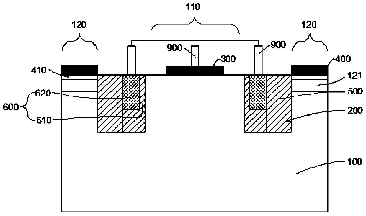
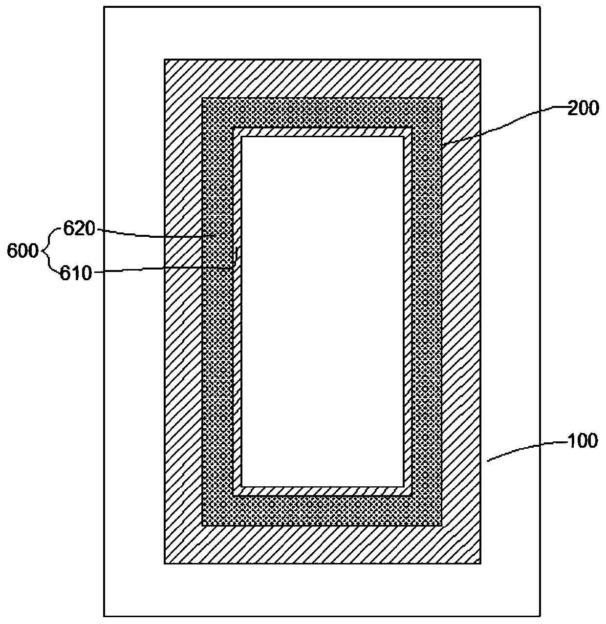
[0025] Such as figure 1 as well as figure 2 As shown, a Schottky diode includes: a semiconductor material 100, a trench 200 separating the semiconductor material 100 into an anode region 110 and a cathode region 120, and an anode metal layer in contact with the semiconductor material 100 on the anode region 110 300, the cathode metal layer 400 in contact with the semiconductor material 100 on the cathode region 120, the trench 200 is in a ring shape, the part of the trench 200 close to the cathode region 120 is filled with an insulating medium 500, and the trench 200 A gate structure 600 is formed near the anode region 110, the gate structure 600 is composed of a first gate insulating layer 610 formed on the inner wall of the trench 200 and conductive polysilicon 620 filled in the trench, the conductive polysilicon 620 and the The anode metal layer 300 is electrically connected.
[0026] Specifically, the semiconductor material 100 may be silicon, silicon carbide, silicon g...
no. 2 example
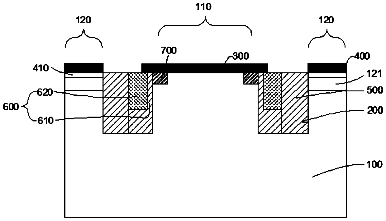
[0032] Such as image 3 As shown, the technical solution of this embodiment is basically the same as that of the first embodiment, the difference is that the anode metal layer 300 is in contact with the conductive polysilicon 620 to realize electrical connection, which can increase the Schottky contact area to a certain extent and reduce the Small forward conduction voltage drop, preferably, an insulating region 700 is formed at the corner formed by the anode metal layer 300 and the groove 200, so as to avoid the top corner formed by the anode metal layer 300 and the groove 200 under reverse voltage. The corner directly contacts the anode metal layer 300 to form a tip discharge and cause reverse leakage.
no. 3 example
[0034] Such as Figure 4 As shown, the technical solution of this embodiment is basically the same as that of the first embodiment, the difference is that the conductive polysilicon 620 fills the groove 200, and the height exceeds the surface of the groove opening, and is biased towards the anode region at the groove opening One side of 110 expands outwards, so that the width of the conductive polysilicon 620 outside the trench 200 is greater than the width of the conductive polysilicon 620 inside the trench 200, and insulating spacers 800 are formed on both sides of the conductive polysilicon 620 outside the trench 200, and the trench The second gate insulating layer 630 is formed under the conductive polysilicon 620 outside 200. In this embodiment, the gate structure 600 is extended to the side of the anode region 110, so that under the reverse voltage, the gate structure 600 realizes the semiconductor material from two directions. The depletion of 100 further enhances the r...
PUM
 Abstract
Description
Claims
Application Information


