GaN HMET device with gradually-change fluorine ion terminal in passivation layer

A fluoride ion, passivation layer technology, applied in semiconductor devices, electrical components, circuits, etc., can solve problems affecting 2DEG transport characteristics, device performance degradation, etc., to achieve low forward conduction resistance, high withstand voltage, high reliability sexual effect

Active Publication Date: 2021-05-28
UNIV OF ELECTRONICS SCI & TECH OF CHINA
View PDF9 Cites 1 Cited by
  • Summary
  • Abstract
  • Description
  • Claims
  • Application Information

AI Technical Summary

Problems solved by technology

[0003] In a conventional HEMT structure with fluorine-implanted terminations, the implantation of fluorine ions into the thinner AlGaN barrier layer will affect the transport properties of 2DEG, leading to device performance degradation

Method used


Image

  • GaN HMET device with gradually-change fluorine ion terminal in passivation layer
  • GaN HMET device with gradually-change fluorine ion terminal in passivation layer
  • GaN HMET device with gradually-change fluorine ion terminal in passivation layer

Examples


Embodiment 1

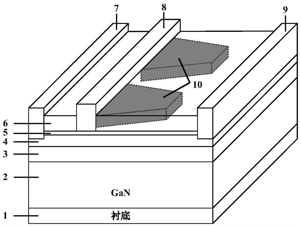
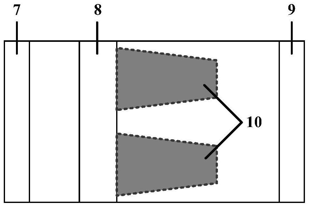
[0026] Such as figure 1 As shown, the HEMT device of this example includes a substrate layer 1, a GaN buffer layer 2, a channel layer 3, a barrier layer 4, a top GaN layer 5, and a passivation layer 6, which are sequentially stacked from bottom to top along the vertical direction of the device. ; Along the lateral direction of the device, the surface of the device has a source structure, a gate structure, a fluorine ion implantation terminal 10 and a drain structure in the passivation layer from one side to the other, and the source structure and the drain structure are located in the device both ends of the upper surface;

[0027] The source structure extends through the passivation layer 6 and the top GaN layer 5 to the barrier layer 4 along the vertical direction of the device, and the source structure is composed of a first conductive material 7; the upper surface of the first conductive material 7 leads to the source ; The source structure is an ohmic contact;

[0028] ...

Embodiment 2

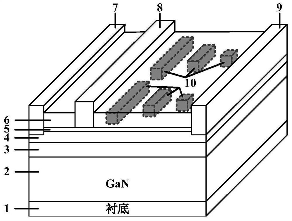
[0033] The difference between this example and Example 1 is that in this example, a GaNHMET device with a passivation layer graded fluorine ion terminal, along the longitudinal direction of the device, the fluorine ion implantation terminal 10 is divided into multiple parts with the same shape but different Each of the continuous trapezoidal regions includes a plurality of parallel and intermittently separated rectangular fluorine ion implantation strips along the lateral direction of the device, and the area of ​​the rectangular fluorine ion implantation strips decreases successively along the direction from the gate structure to the drain structure. Compared with implementation case 1, the advantage of this example is that the total area of ​​fluorine ion implantation is reduced, and the depletion effect on channel electrons is reduced, but it still has an obvious regulation effect on the surface electric field of the device.

Embodiment 3

[0035] The difference between this example and Example 1 is that in this example, a GaNHMET device with a passivation layer graded fluorine ion terminal, along the longitudinal direction of the device, the fluorine ion implantation terminal 10 is divided into multiple parts with the same shape but different The continuous trapezoidal regions are along the direction from the gate structure to the drain structure, and each region is an irregular region distributed in a step shape as the fluorine ion implantation area is equally spaced and gradually decreased.


PUM


Abstract

The invention belongs to the technical field of power semiconductors, and relates to a GaN HMET device with a gradually-change fluorine ion terminal in a passivation layer. The GaN HMET device is mainly characterized in that a fluorine ion implantation terminal structure is introduced between a grid and a drain of the device, and the area of a fluorinion injection region is gradually reduced from the side, close to the grid, to the side of the drain, so an electric field peak of the edge of the grid is effectively reduced, and a new electric field peak is introduced into the middle of a drift region to modulate a transverse electric field of the device; and the fluorine ion implantation terminal structure is located in the thick passivation layer, so physical damage of ion implantation to an AlGaN material and influence of ion implantation to 2DEG mobility can be avoided, device characteristics are improved, and current collapse is inhibited. The beneficial effect of the invention is that the structure can realize higher withstand voltage and smaller specific on-resistance.

Description

technical field [0001] The invention belongs to the technical field of power semiconductors, and in particular relates to a GaN HMET device with a passivation layer graded fluorine ion terminal. Background technique [0002] HEMTs based on GaN materials have broad application prospects in the fields of high-current, low-power, and high-voltage switching devices. For AlGaN / GaN HEMT devices, due to the presence of electric field spikes at the gate edge, excessive leakage current, etc., the device breaks down early, and its withstand voltage is far from the theoretical limit of GaN materials. The fluorine ion implantation terminal can reduce the electric field peak at the edge of the gate and introduce a new electric field peak, which can effectively improve the withstand voltage of the device. In particular, the gradiently doped fluorine ion implanted terminal can improve the device surface field more effectively. However, fluoride ion implantation is unstable and limited by...

Claims


Application Information

Patent Timeline
Patent Type & Authority Applications(China)
IPC IPC(8): H01L29/778
CPCH01L29/778H01L29/7786
Inventor 魏杰邓思宇郗路凡孙涛贾艳江廖德尊张成罗小蓉
Owner UNIV OF ELECTRONICS SCI & TECH OF CHINA
Why Eureka
Try Eureka