Hybrid Schottky barrier diode structure with P-type nickel oxide material

A Schottky potential, hybrid technology, applied in semiconductor devices, electrical components, circuits, etc., can solve the problems of narrow current channel, high breakdown voltage, increase forward conduction resistance of devices, etc., to reduce forward conduction Resistance, large forward current density, solving the effect of difficult acquisition

Active Publication Date: 2021-06-04
HEBEI UNIV OF TECH
View PDF6 Cites 1 Cited by
  • Summary
  • Abstract
  • Description
  • Claims
  • Application Information

AI Technical Summary

Problems solved by technology

However, for wide-bandgap semiconductors, the further development of TJBS is limited by the lack of effective P-type dopant ions, low activation rate of P-type impurities, and high activation annealing temperature.
Although the trench MOS device structure can well avoid the shortcomings of the junction barrier Schottky diode structure and achieve a high breakdown voltage, the electric field concentration at the corner of the trench becomes the main factor limiting its structure to obtain ideal breakdown characteristics. factor
In addition, for the above two device structures, although the reverse characteristics are greatly improved compared with the traditional planar SBD, that is, higher breakdown voltage and lower leakage current, but due to the narrow current channel, when the device When it is in forward bias, it is easy to cause current crowding at the corner of the mesa, thereby increasing the forward conduction resistance of the device and reducing the forward current density of the device to a large extent, which in turn causes the degradation of the forward characteristics of the device

Method used


Image

  • Hybrid Schottky barrier diode structure with P-type nickel oxide material
  • Hybrid Schottky barrier diode structure with P-type nickel oxide material
  • Hybrid Schottky barrier diode structure with P-type nickel oxide material

Examples


Embodiment 1

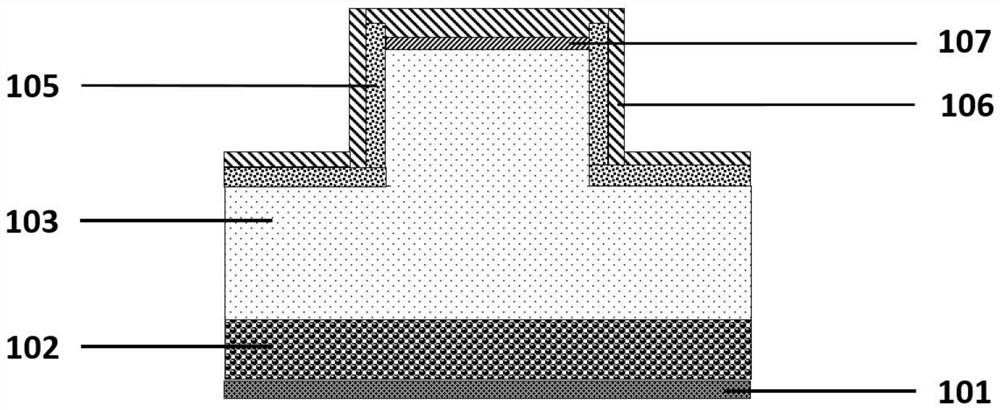
[0060] This embodiment adopts the structure of a hybrid Schottky barrier diode with p-type nickel oxide (p-NiO) material as image 3 shown. The device structure along the epitaxial direction is as follows: bottom ohmic contact electrodes 101, N + Substrate 102, N - drift layer 103, wherein, N - The drift layer 103 has protrusions arranged in an array, a single protrusion is a middle protrusion, a step structure, and the projected area of ​​the protrusion part is all N - 35% of the area of ​​the drift layer 103; the N of the raised part - On the drift layer 103 is a Schottky contact electrode 107; the N of the non-protruding part -The drift layer 103 is covered with a p-type layer 104, and the inner side of the upper surface of the p-type layer 104 is a field plate dielectric layer 105 (the projected area of ​​the field plate dielectric layer 105 is 70% of the upper surface of the p-type layer 104), N - The side wall of the raised part of the drift layer 103 is also covere...

Embodiment 2

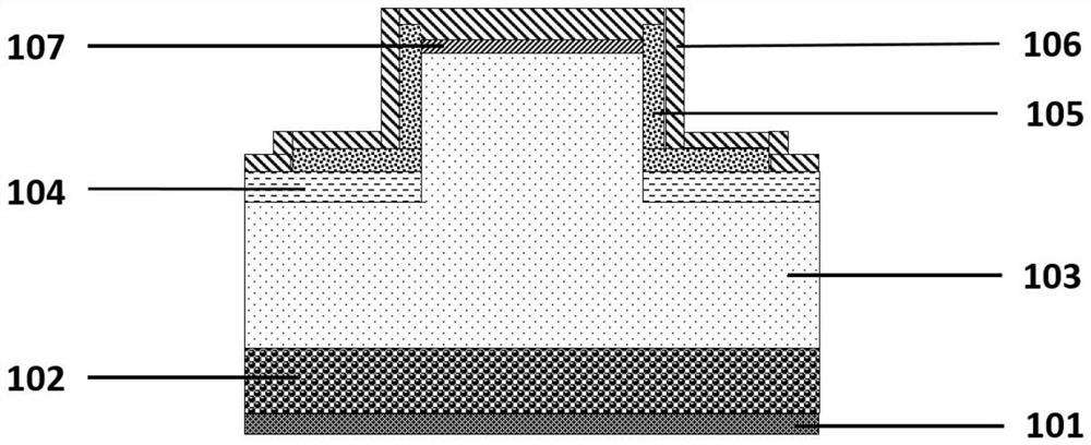
[0090] This embodiment adopts the structure of a hybrid Schottky barrier diode with p-type nickel oxide (p-NiO) material as Figure 6 As shown, the difference between this structure and the structure in Example 1 is that side wall field plate structures are provided on both sides of the p-NiO layer. The sidewall field plate structure is formed after the first ICP dry etching - The outer edges on both sides of the upper surface of the non-protruded part of the drift layer 103 are again subjected to ICP dry etching to form a second shallow step structure on the outer surface. The device structure along the epitaxial direction is as follows: bottom ohmic contact electrodes 101, N + Substrate 102, N - drift layer 103, wherein, N - The drift layer 103 is a two-layer stepped structure with a raised middle, and the area of ​​the lowest groove is the entire N - 25% of the area of ​​the drift layer 103 (that is, the projected area of ​​the two layers of raised parts is all N - 75%...


PUM

PropertyMeasurementUnit
thicknessaaaaaaaaaa
thicknessaaaaaaaaaa
thicknessaaaaaaaaaa

Abstract

The invention relates to a hybrid Schottky barrier diode structure with a P-type nickel oxide material. The structure comprises a bottom ohmic contact electrode, an N+ substrate, an N-drift layer, a groove, a P-type layer, a field plate dielectric layer, field plate metal and a Schottky contact electrode, the N-drift layer is of a step structure, and p-NiO materials are grown on selected areas on the two sides of a table top to replace P-type wide bandgap semiconductor materials. Therefore, the problem that a P-type epitaxial growth technology and an ion implantation technology of a wide bandgap semiconductor material at the present stage are immature can be well solved. The structure is high in operability, low in cost, simple and reliable in process and suitable for industrial application and popularization.

Description

technical field [0001] The invention relates to the field of power electronic devices, in particular to a hybrid Schottky barrier diode structure and a preparation method with p-type nickel oxide (p-NiO) material. Background technique [0002] Power semiconductor devices are also called power electronic devices. With the continuous development of power electronics theory and technology, and under the theme of vigorously advocating energy conservation in the country, power semiconductor devices, as an important part of energy conversion, are rapidly being used in industrial production, electrical equipment, Rail transportation, national defense and military, aerospace, new energy systems, and daily life have received extensive attention and applications. In recent years, wide bandgap semiconductor materials such as SiC, GaN, Ga 2 o 3 etc. have received extensive attention from many researchers, especially the application of GaN power diodes has been fully developed, and gra...

Claims


Application Information

Patent Timeline
Patent Type & Authority Applications(China)
IPC IPC(8): H01L29/06H01L29/24H01L29/872
CPCH01L29/872H01L29/0684H01L29/0619H01L29/0623H01L29/24
Inventor 张紫辉黄福平张勇辉楚春双
Owner HEBEI UNIV OF TECH
Why Eureka
Try Eureka