

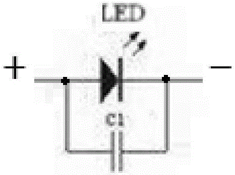
Light-emitting diode (LED) chip with capacitance structure and preparation method thereof
A technology of LED chip and capacitor structure, which is applied in the direction of circuits, electrical components, semiconductor devices, etc., can solve problems such as visual impact, chip light emission is not constant, and the light source cannot be guaranteed to be stable without flickering, so as to improve reliability and control generation Cost, the effect of preventing surge impact
- Summary
- Abstract
- Description
- Claims
- Application Information
AI Technical Summary
Problems solved by technology
Method used
Image

Examples
Embodiment Construction
[0039] In order to enable those skilled in the art to better understand the technical solutions in the present invention, the technical solutions in the embodiments of the present invention will be clearly and completely described below in conjunction with the drawings in the embodiments of the present invention. Obviously, the described The embodiments are only some of the embodiments of the present invention, not all of them. Based on the embodiments of the present invention, all other embodiments obtained by persons of ordinary skill in the art without making creative efforts shall fall within the protection scope of the present invention.
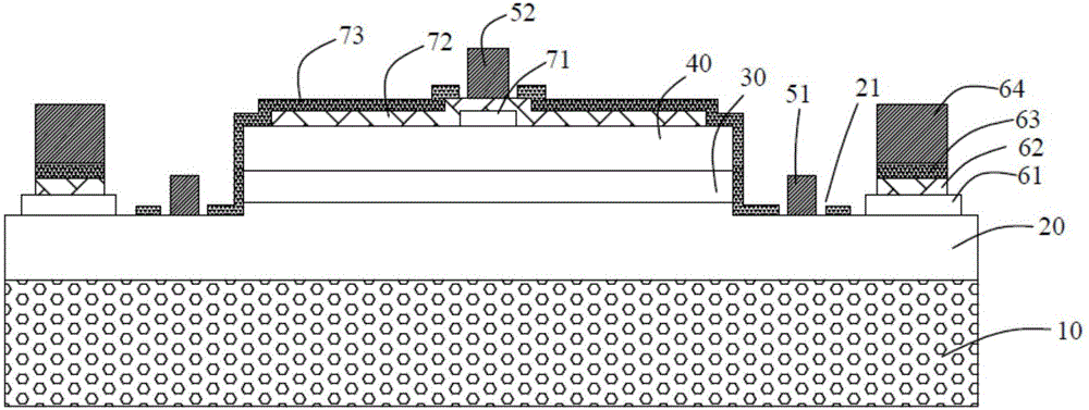
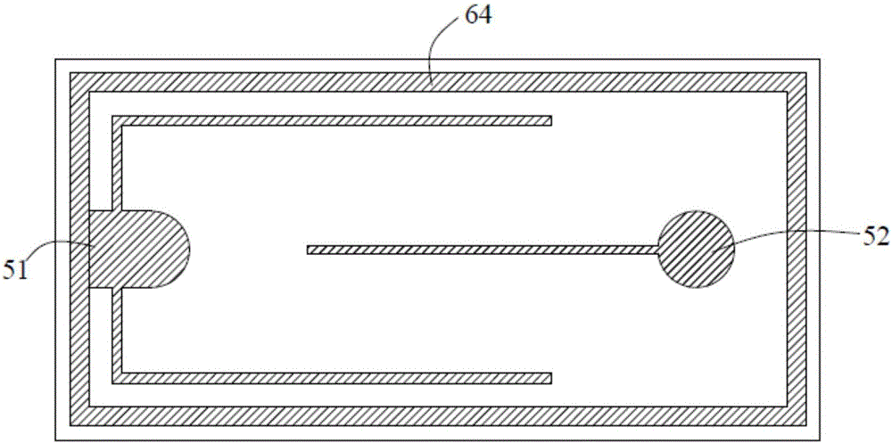
[0040] The invention discloses an LED chip with a capacitor structure. The LED chip comprises: an N-type semiconductor layer, a multi-quantum well light-emitting layer, a P-type semiconductor layer, an N electrode and a P electrode, and the N electrode is electrically connected to the N-type semiconductor layer. connected, the P electro...
PUM
 Abstract
Description
Claims
Application Information