Conductive nanowire layer and graphical method and application thereof

A conductive nano-patterning technology, applied in circuits, electrical components, semiconductor devices, etc., can solve the problems of metal layer and substrate falling off, cumbersome patterning methods, etc., and achieve the effect of uniform light

Active Publication Date: 2017-05-31
CHENGDU VISTAR OPTEOLECTRONICS CO LTD
View PDF9 Cites 7 Cited by
  • Summary
  • Abstract
  • Description
  • Claims
  • Application Information

AI Technical Summary

Problems solved by technology

[0004] The technical problem to be solved by the present invention is that the patterning method of nano conductive materials in the prior art is cumbersome and easily leads to the problem that the metal layer and the substrate fall off, thereby providing a patterning method of the conductive nanowire layer. The material is mixed with the patterning glue photoresist, and only one step of curing is needed to realize the patterning of the nanowire material, and the bonding force between the conductive nanowire layer and the substrate is strong, and it is not easy to fall off

Method used


Image

  • Conductive nanowire layer and graphical method and application thereof
  • Conductive nanowire layer and graphical method and application thereof
  • Conductive nanowire layer and graphical method and application thereof

Examples


Embodiment 1-4

[0042] The patterning method of the conductive nanowire layer in this embodiment is as follows:

[0043] The conductive nanowire material and the photoresist are uniformly mixed to form a mixed solution, the mixed solution is coated on the substrate and then exposed for an exposure time of 1-120s, after curing, forming, and developing to obtain a conductive nanowire layer. Coating adopts spin coating or blade coating.

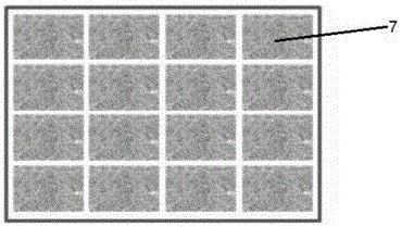
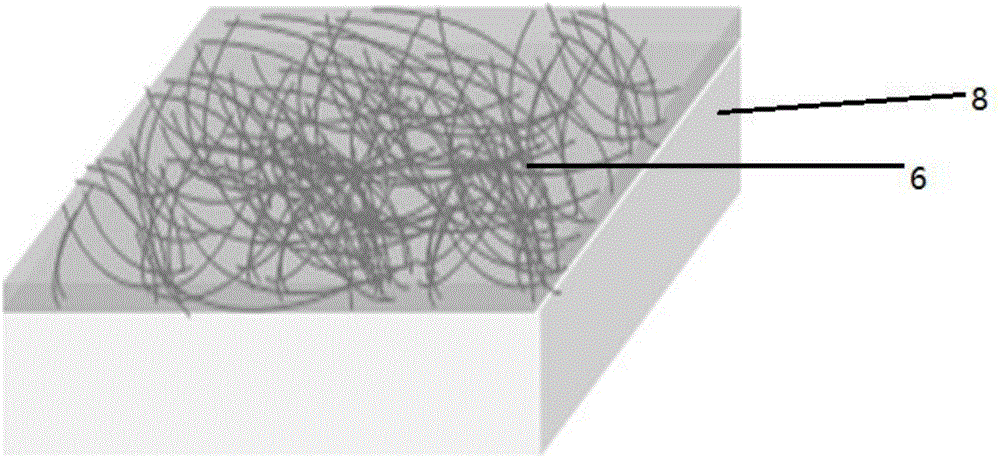
[0044] Different exposure masks can be used to obtain conductive nanowire layers with different patterns after exposure and development, such as image 3 In the regularly arranged conductive nanowire layer 7. Light passing through Figure 5 After the exposed area 21 of the middle mask is irradiated with the mixed solution in the corresponding area to cure it, the non-exposed area 22 can block the light, and the mixed solution in the corresponding area does not cure and is removed by washing.

[0045] Table 1 Process condition parameter table of the patterning method ...

Embodiment 5-8

[0052] The patterning method of the conductive nanowire layer in this embodiment is as follows:

[0053] The conductive nanowire material and the ultraviolet curing adhesive are patterned by uniformly mixing the conductive nanowire material and the ultraviolet curing adhesive to form a mixed solution, and the mixed solution is coated on the substrate and then cured by ultraviolet light After molding, a conductive nanowire layer is obtained. Coating adopts spin coating or blade coating.

[0054] Different exposure masks can be used to obtain conductive nanowire layers with different patterns after exposure and development, such as image 3 In the regularly arranged conductive nanowire layer 7. Light passing through Figure 5 After the exposed area 21 of the middle mask is irradiated with the mixed solution in the corresponding area to cure it, the non-exposed area 22 can block the light, and the mixed solution in the corresponding area does not cure and is removed by washing.

[005...

Embodiment 9-12

[0062] The patterning method of the conductive nanowire layer in this embodiment is as follows:

[0063] The conductive nanowire material and the thermal curing glue are uniformly mixed to form a mixed solution, and the mixed solution is coated on the substrate, and then heated and cured to form a mixed solution. Coating adopts spin coating or blade coating.

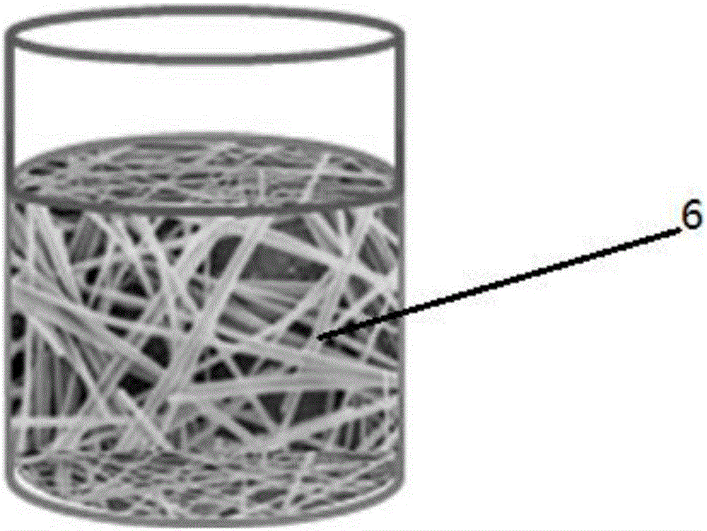
[0064] Different heat curing templates can be used such as Image 6 The heating mask shown is heated and cured to obtain conductive nanowire layers with different patterns, such as image 3 In the regularly arranged conductive nanowire layer 7. During the heating and curing process, the mixed solution coating in the area corresponding to the heating area 11 is heated and cured to form a conductive nanowire layer, and the mixed solution corresponding to the non-heating area 12 is not cured and is removed by washing.

[0065] Table 3 Process condition parameter table of the patterning method in Examples 9-12

[0066] Serial ...


PUM

PropertyMeasurementUnit
thicknessaaaaaaaaaa

Abstract

The invention provides a graphical method of a conductive nanowire layer. The method comprises the steps that a conductive nanowire material and graphical glue are mixed to form a mixed solution, a substrate is coated with the mixed solution, and then the conductive nanowire layer is obtained through curing molding. The conductive nanowire layer can be obtained just through one step of curing. Compared with a traditional method, etching and stripping technologies are omitted, and the adhesive force between the nanometer conductive material and the substrate is enhanced; when the conductive nanowire layer is used as an electrode layer of an organic electroluminescence device, light rays of the device are uniform, and the problem of visual light ray non-uniformity or other optical defects cannot be generated.

Description

Technical field [0001] The invention belongs to the technical field of organic electroluminescent devices, and specifically relates to a patterning method of a conductive nanowire layer and a high-resolution OLED device containing the conductive nanowire layer. Background technique [0002] Metal nanowires are being studied extensively, and how to realize the patterning of nanowires simply and efficiently is one of the hot spots. The current common practice is to use the process route of film formation, photolithography, and etching to realize patterning of metal nanowire materials. In this way, the process is relatively complicated, which brings about process instability and cost increase. [0003] CN104966588A A method for preparing a nano-scale metal grid transparent conductive film, comprising the following steps: 1) forming a metal film on a substrate; 2) coating a layer of ultraviolet light sensitive photolithography on the metal film In the photoresist, nanowires are rando...

Claims


Application Information

Patent Timeline
Patent Type & Authority Applications(China)
IPC IPC(8): H01L51/56H01L51/50H01L51/52
CPCH10K50/00H10K50/805H10K71/00
Inventor 李阳邓亮陶国胜张成明刘晓佳王雷
Owner CHENGDU VISTAR OPTEOLECTRONICS CO LTD
Why Eureka
Try Eureka