Check patentability & draft patents in minutes with Patsnap Eureka AI!

GaN-based light-emitting diode and manufacturing method thereof

A light-emitting diode, gallium nitride-based technology, applied in semiconductor devices, electrical components, circuits, etc., can solve problems such as poor hole injection efficiency, and achieve the effect of improving radiation recombination efficiency

Active Publication Date: 2018-11-02
XIAMEN SANAN OPTOELECTRONICS CO LTD
View PDF4 Cites 0 Cited by
  • Summary
  • Abstract
  • Description
  • Claims
  • Application Information

AI Technical Summary

Problems solved by technology

However, there is also a certain amount of hole injection in the non-V-type defect region (C-plane), and the hole injection efficiency in this region is poor

Method used


Image

  • GaN-based light-emitting diode and manufacturing method thereof
  • GaN-based light-emitting diode and manufacturing method thereof
  • GaN-based light-emitting diode and manufacturing method thereof

Examples


Embodiment Construction

[0037] The light-emitting diode of the present invention and its manufacturing method are described in detail below in conjunction with schematic diagrams, so as to fully understand and implement the realization process of how to apply technical means to solve technical problems and achieve technical effects in the present invention. It should be noted that, as long as there is no conflict, each embodiment and each feature in each embodiment of the present invention can be combined with each other, and the formed technical solutions are all within the protection scope of the present invention.

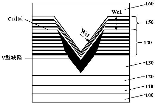
[0038] figure 1 A gallium nitride-based light-emitting diode with a conventional structure is shown, including: a growth substrate 100, a buffer layer 110, an n-type gallium nitride layer 120, an InGaN / GaN superlattice structure 130, and a multi-quantum well active layer 140 Layer, p-type AlGaN / InGaN electron blocking layer 150 and p-type gallium nitride layer 160, wherein the multi-qu...


PUM


Abstract

A gallium nitride-based light emitting diode and a manufacturing method therefor, wherein the structure sequentially comprises: an n-type nitride layer (120), an active layer (140), an Alx1In(1-x1)N / Inx2Ga(1-x2)N superlattice electron blocking layer (150), and a p-type nitride layer (160); a surface of the active layer (140) is provided thereon with a V-type defect and a plane area, which is connected to the V-type defect, the Alx1In(1-x1)N / Inx2Ga(1-x2)N electron blocking layer (150) is formed at the plane area and extends to a sidewall area of the V-type defect; when a current is injected, holes are injected into the active layer (140) from a V-type defect position, and electrons are blocked at the plane area such that the same stay at the active layer (140).

Description

technical field [0001] The invention belongs to the field of semiconductor lighting, and in particular relates to a gallium nitride-based light-emitting diode and a manufacturing method thereof. Background technique [0002] Gallium nitride-based light-emitting diodes (Light Emitting Diodem, referred to as LED) have been widely used in various light source fields such as backlighting, lighting, car lights, and decorations due to their high luminous efficiency. Further improving the luminous efficiency of LEDs is still the focus of current industry development. The luminous efficiency is mainly determined by two factors. The first is the radiative recombination efficiency of electrons and holes in the active region, that is, the internal quantum efficiency; the second is the light extraction efficiency. Techniques to improve these two efficiencies have been widely reported. In terms of improving the internal quantum efficiency, such as quantum well energy band design, impro...

Claims


Application Information

Patent Timeline
Patent Type & Authority Patents(China)
IPC IPC(8): H01L33/04H01L33/06H01L33/14H01L33/00
CPCH01L33/00H01L33/007H01L33/0075H01L33/04H01L33/06H01L33/145
Inventor 陈秉扬张中英罗云明黄文嘉陈福全叶孟欣
Owner XIAMEN SANAN OPTOELECTRONICS CO LTD
Features
  • R&D
  • Intellectual Property
  • Life Sciences
  • Materials
  • Tech Scout
  • Unparalleled Data Quality
  • Higher Quality Content
  • 60% Fewer Hallucinations
Learn More