Manufacturing method of fine circuit board free of corrosion resistant layer

A manufacturing method and circuit board technology, applied in the directions of printed circuit manufacturing, printed circuits, electrical components, etc., can solve problems such as difficulties and inapplicability to fine circuits, and achieve the effect of avoiding side erosion of circuits and good quality of circuit manufacturing.

Inactive Publication Date: 2017-06-13
YIXING SILICON VALLEY ELECTRONICS TECH
View PDF5 Cites 8 Cited by
  • Summary
  • Abstract
  • Description
  • Claims
  • Application Information

AI Technical Summary

Problems solved by technology

[0006] Because the line side etching has brought great difficulties to the refinement of printed circuit board graphics, yield improvement and i...

Method used


Image

  • Manufacturing method of fine circuit board free of corrosion resistant layer
  • Manufacturing method of fine circuit board free of corrosion resistant layer
  • Manufacturing method of fine circuit board free of corrosion resistant layer

Examples


Embodiment 1

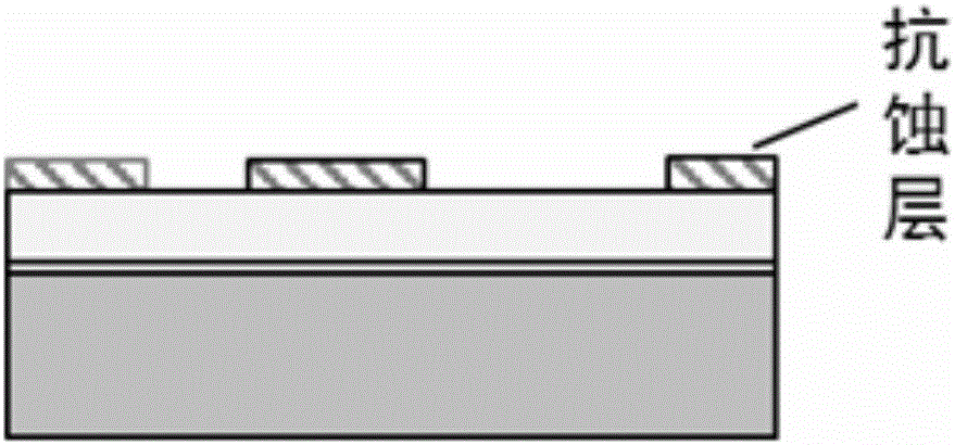
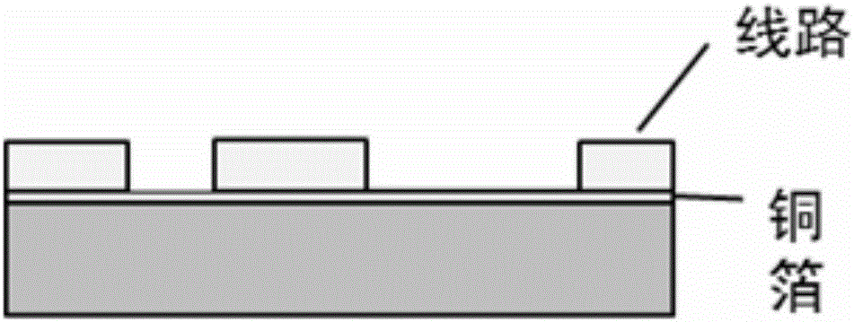
[0030] The method for manufacturing a fine circuit board without a resist layer provided in this embodiment includes the following processes: lamination-thinning of base copper-drilling-drilling-copper pre-plating-pattern electroplating-film fading flash etching-subsequent process, wherein :

[0031] (1) In this embodiment, a thin copper foil with a copper thickness ≤ 12 μm is selected for lamination during the production process of the circuit board;

[0032] (2) Thinning the base copper process on the copper surface on the plate so that the thickness of the copper surface is uniformly reduced to 5-7μm. The potion used in the base copper thinning process is a mixed system of copper thinning agent, sulfuric acid, and hydrogen peroxide;

[0033] Control the thinned copper thickness. When there are through holes in the plate structure, the copper thickness of the thinned copper is controlled at 5 μm; when there are blind holes and through holes in the plate, the copper thickness...


PUM

PropertyMeasurementUnit
Copper thicknessaaaaaaaaaa
Thicknessaaaaaaaaaa
Resolutionaaaaaaaaaa

Abstract

The invention discloses a manufacturing method of a fine circuit board free of a corrosion resistant layer. The method comprises the processes of laminating, base copper reduction, drilling, depositing copper preplating, pattern electroplating, stripping and flash rusting and subsequent processes. According to the manufacturing method, the fine circuit board is manufactured by combining a thin copper foil with a flash rusting technology; the manufacturing method can be used for manufacturing an ultrafine circuit; and the manufacturing accuracy of the circuit is improved.

Description

technical field [0001] The invention relates to a method for manufacturing a circuit board, in particular to a method for manufacturing a fine circuit board without a resist layer. Background technique [0002] With the rapid development of electronic products towards multi-function, miniaturization, and light weight, the requirements for printed circuit boards are becoming more and more high-density, high-integrated, and miniaturized. Fine circuit manufacturing is the key technology for PCB development. The degree of modernization has gradually shifted from the millimeter-level macro scale to the sub-micro and micro-micro scale, and fine lines ≤ 3 / 3mil will become the mainstream. In BOT-type fcCSP packaging substrates with stepped Cavity solder resist structures, optical The optoelectronic panels used in the module communication system have higher requirements for circuit accuracy. [0003] The current mainstream production methods in the industry include two etching proce...

Claims


Application Information

Patent Timeline
IPC IPC(8): H05K3/10
CPCH05K3/108H05K2203/0353
Inventor 石靖李俊明桂芳
Owner YIXING SILICON VALLEY ELECTRONICS TECH
Why Eureka
Try Eureka