Supercharge Your Innovation With Domain-Expert AI Agents!

Transistor and method of forming the same

A technology of transistors and doped layers, applied in semiconductor devices, semiconductor/solid-state device manufacturing, electrical components, etc., can solve problems affecting device performance, transistor junction leakage, etc., to improve reliability, increase distance, and avoid gate electrodes. Effects of Current and Substrate Current

Active Publication Date: 2020-06-09
SEMICON MFG INT (SHANGHAI) CORP +1
View PDF6 Cites 0 Cited by
  • Summary
  • Abstract
  • Description
  • Claims
  • Application Information

AI Technical Summary

Problems solved by technology

[0005] However, the transistors formed by this method still have the problem of junction leakage, which affects the performance of the formed devices.

Method used


Image

  • Transistor and method of forming the same
  • Transistor and method of forming the same
  • Transistor and method of forming the same

Examples


Embodiment Construction

[0040] It can be seen from the background art that the transistors in the prior art have the problem of junction leakage. Now combine the structure of the transistor to analyze the cause of the junction leakage problem:

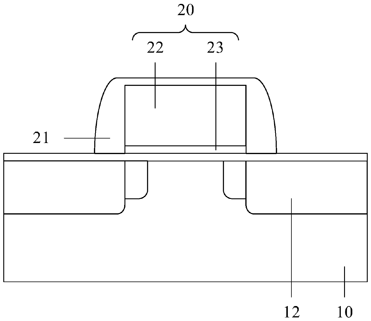
[0041] refer to figure 1 , shows a schematic structural diagram of a transistor in the prior art.

[0042] The step of forming an ultra-shallow junction transistor includes: forming a gate structure 20 on the semiconductor substrate 10, the gate structure 20 including a gate electrode 22 and a gate dielectric layer 23; doping implantation, and diffuse the implanted ions in the semiconductor substrate 10 through an annealing process; form gate spacers 21 located on the sidewalls of the gate structure 20; conduct high-energy The heavily doped is implanted to form a source region or a drain region 12 .

[0043] Due to the blocking effect of the gate spacer 21 , the region of the semiconductor substrate 10 below the gate spacer 21 is still a lightly doped regi...


PUM

PropertyMeasurementUnit
thicknessaaaaaaaaaa
thicknessaaaaaaaaaa

Abstract

The invention provides a transistor and a forming method thereof. The forming method comprises: a substrate is provided and a gate structure is formed on the surface of the substrate; a first doped layer is formed in the substrate at the two sides of the gate structure; a first side wall is formed at the side wall of the gate structure; the first doped layer at the two sides of the first side wall are removed; a second doped layer is formed in the substrate at the two sides of the first sidewall, wherein the doping concentration of the second doped layer is higher than the doping concentration of the first doped layer; a second side wall is formed at the side wall of the first side wall; and a source region or a drain region is formed in the substrate at the two sides of the second side wall. According to the transistor and the forming method thereof, because the first doping layer and the second doping layer are arranged and the doping concentration of the second doped layer is higher than the doping concentration of the first doped layer, the distance between the gate structure and the channel is increased, the distance between the gate dielectric layer and the channel carrier is increased, the possibility of injection of hot carriers into the gate dielectric layer is reduced, formation of gate currents and substrate currents is avoided, the performance of the transistor is improved, and the reliability of the device is enhanced.

Description

technical field [0001] The invention relates to the field of semiconductor manufacturing, in particular to a transistor and a forming method thereof. Background technique [0002] In semiconductor devices, transistors are an important basic device. The basic structure of a transistor includes three main areas: source (Source), drain (Drain) and gate (Gate). Wherein the source and drain are formed by high doping. According to different device types, it can be divided into N-type doping (NMOS) and P-type doping (PMOS). [0003] With the development of integrated circuits to ultra-large-scale integrated circuits, the circuit density inside the integrated circuit is increasing, and the number of components contained in the integrated circuit is also increasing, and the size of the components is also reduced. As the size of the MOS device decreases, the channel of the MOS device shortens accordingly. Due to the shortening of the channel, the slow-changing channel approximatio...

Claims


Application Information

Patent Timeline
Patent Type & Authority Patents(China)
IPC IPC(8): H01L21/336H01L29/78H01L29/06H01L29/36
CPCH01L29/0688H01L29/36H01L29/66477H01L29/6656H01L29/78
Inventor 赵猛
Owner SEMICON MFG INT (SHANGHAI) CORP
Features
  • R&D
  • Intellectual Property
  • Life Sciences
  • Materials
  • Tech Scout
  • Unparalleled Data Quality
  • Higher Quality Content
  • 60% Fewer Hallucinations
Learn More