Microelectronic package lead frame in matrix form

A technology for encapsulating leads and microelectronics, applied in circuits, electrical components, electrical solid devices, etc., can solve the problems of poor lead frame precision, low density, lack of refinement of external pins, etc., to improve the processing level and promote renewal. replacement effect

Inactive Publication Date: 2017-06-20
广东先捷电子股份有限公司
View PDF0 Cites 3 Cited by
  • Summary
  • Abstract
  • Description
  • Claims
  • Application Information

AI Technical Summary

Problems solved by technology

[0006] The purpose of this invention patent is to overcome the poor precision of the lead frame, low density, low output, lack of refinement of the outer pins of the plug-in components in the manufacturing process of the existing similar products, and the outer pins are too long and too wide. , t

Method used


Image

  • Microelectronic package lead frame in matrix form
  • Microelectronic package lead frame in matrix form

Examples


Example Embodiment

[0022] The present invention will be further explained in detail below in conjunction with the examples, and the examples are only for explanation and are not intended to limit the present invention.

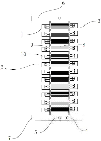
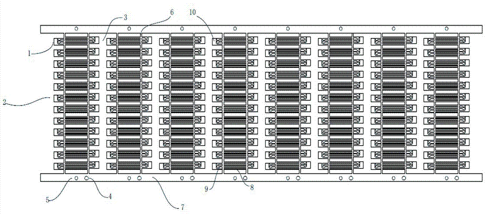
[0023] like figure 2 As shown, a matrix-arranged microelectronic package lead frame according to an embodiment of the present invention, the lead frame as a whole includes a package window unit (1), a package array unit (2), a cross-symmetrical unit (3), and process calibration holes (4 ), mechanical transmission positioning holes (5), connecting middle ribs (6), and lateral positioning guiding main ribs (7); the package array unit (2) is composed of a basic package window unit (1), and the cross-symmetrical unit (3) It is composed of the package array unit (2) rotated and connected, the connecting rib (6) plays a role in connecting and fixing the package window unit (1), package array unit (2) and cross-symmetrical unit (3), and the lateral positioning guide The main reinforc...


PUM

PropertyMeasurementUnit
Thicknessaaaaaaaaaa
Thicknessaaaaaaaaaa
Widthaaaaaaaaaa

Abstract

The invention relates to the technical field of manufacturing semiconductor electronic components, in particular to a matrix-arranged microelectronic packaging lead frame. The lead frame includes a packaging window unit (1), a packaging array unit (2), a cross-symmetrical unit (3), a process calibration hole (4), a mechanical transmission positioning hole (5), a connecting rib (6), and a lateral positioning guide main rib ( 7) Composition; it overcomes the poor precision of the lead frame, low density, low output, lack of refinement of the outer pins of the plug-in components in the manufacturing process of the existing similar products, and the outer pins are too long and too wide , too thick and other defects, improve the packaging level of the semiconductor industry, promote the update and iteration of equipment, expand the overall structure according to the manufacturing requirements of semiconductor components, and achieve the optimal production plan and efficiency. The invention can be widely used in the industrial market and consumption The supply of semiconductor electronic components such as electronics is gradually developing towards high precision, high density and high output.

Description

technical field [0001] The invention relates to the technical field of manufacturing semiconductor electronic components, in particular to a matrix-arranged microelectronic packaging lead frame. Background technique [0002] In the post-production process of semiconductor electronic components, lead frames are indispensable; electronic technology is changing with each passing day, electronic products are constantly being updated, and the IT industry is developing at a high speed. This is what each of us can feel in our daily life and work. Things; the pins of electronic products bought in the electronic market look neat and regular and arranged in an orderly manner. The design makes people feel that it can be easily installed on the circuit board. The lead frame is used to install integrated circuit chips. The carrier is a key structural component that realizes the electrical connection between the lead-out end of the chip's internal circuit and the outer lead by means of a ...

Claims


Application Information

Patent Timeline
IPC IPC(8): H01L23/495
CPCH01L23/49541
Inventor 郑烽
Owner 广东先捷电子股份有限公司
Why Eureka
Try Eureka