Array substrate and manufacturing method therefor

A technology of an array substrate and a manufacturing method, which is applied in the display field and can solve problems such as incompatibility

Inactive Publication Date: 2017-06-20
XIAMEN TIANMA MICRO ELECTRONICS
View PDF4 Cites 62 Cited by
  • Summary
  • Abstract
  • Description
  • Claims
  • Application Information

AI Technical Summary

Problems solved by technology

[0005] In view of this, an embodiment of the present invention provides an array substrate and a manufacturing method to solve the problem of incompatibility between the layers of the two types of thin film transistors when the metal oxide thin film transistor and the low-temperature polysilicon thin film transistor are simultaneously formed in the display panel, and improve the performance of the array substrate. Electrical performance and stability of display panels

Method used


Image

  • Array substrate and manufacturing method therefor
  • Array substrate and manufacturing method therefor
  • Array substrate and manufacturing method therefor

Examples


Embodiment Construction

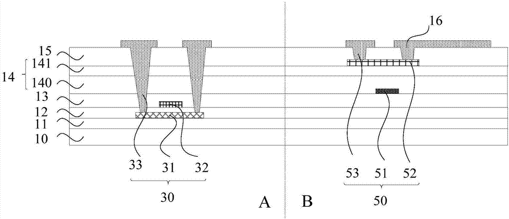
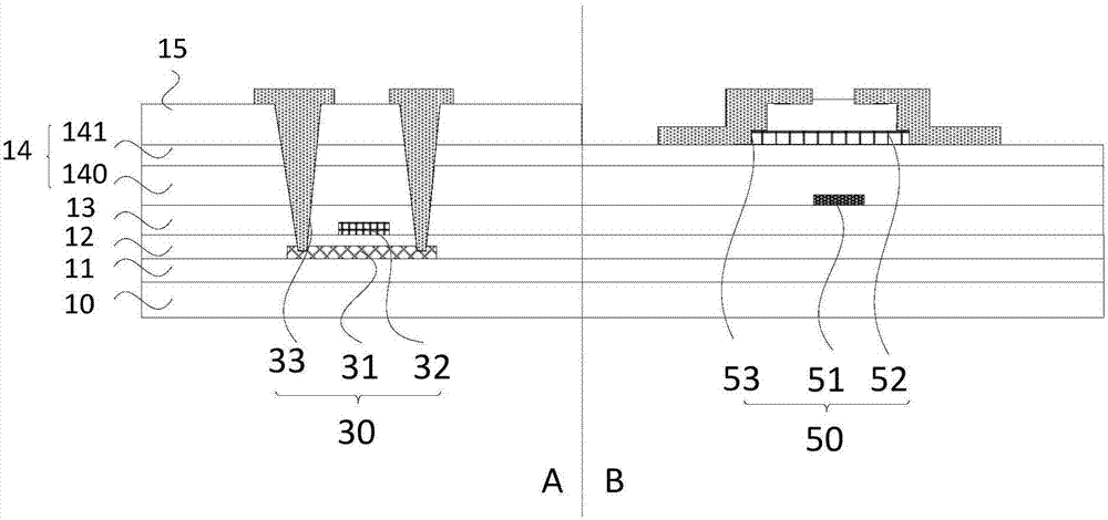
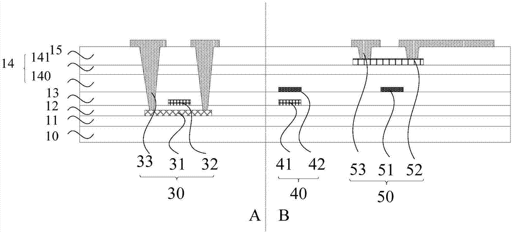
[0024] The present invention will be further described in detail below in conjunction with the accompanying drawings and embodiments. It should be understood that the specific embodiments described here are only used to explain the present invention, but not to limit the present invention. In addition, it should be noted that, for the convenience of description, only some structures related to the present invention are shown in the drawings but not all structures.

[0025] The present invention provides an array substrate, including a base substrate, a plurality of first thin film transistors and a plurality of second thin film transistors; the first thin film transistors and the second thin film transistors are formed above the base substrate; the first thin film transistors The active layer is low temperature polysilicon, the active layer of the second thin film transistor is oxide semiconductor; the first thin film transistor is located in the peripheral circuit area of ​​t...


PUM


Abstract

Embodiments of the invention disclose an array substrate and a manufacturing method therefor. The array substrate comprises a plurality of first thin film transistors and a plurality of second thin film transistors; the first thin film transistors and the second thin film transistors are formed above a substrate; the active layer of each first thin film transistor is low-temperature polysilicon; the active layer of each second thin film transistor is an oxide semiconductor; the first thin film transistors are positioned in a peripheral circuit region of the array substrate; the second thin film transistors are positioned in a display region of the array substrate; the grid electrodes of the first thin film transistors and the second thin film transistors are positioned on different layers; and the source and drain electrodes of the first thin film transistors and the source and drain electrodes of the second thin film transistors are positioned on the same layer. By adoption of the array substrate and the manufacturing method therefor, the problem of incompatibility of two film layers of two types of thin film transistors when the metal oxide thin film transistors and the low-temperature polysilicon thin film transistors are formed in a display panel at the same time is solved, so that the electrical performance and the stability of the display panel are improved.

Description

technical field [0001] Embodiments of the present invention relate to the field of display technology, and in particular to an array substrate and a manufacturing method. Background technique [0002] The metal oxide thin film transistor uses a metal oxide semiconductor layer as the active layer material of the thin film transistor. Due to its high carrier mobility, low deposition temperature and high transparency, it has become the mainstream display panel driving technology. Low-temperature polysilicon thin-film transistors have high switching speeds, and thin-film circuits can be made thinner and smaller, with lower power consumption and so on. [0003] In the prior art, low-temperature polysilicon thin film transistors are used in the peripheral circuit area, and metal oxide thin film transistors are used in the pixel drive circuit in the display area, which improves the problems of poor device uniformity and leakage current. [0004] However, due to the current manufac...

Claims


Application Information

Patent Timeline
Patent Type & Authority Applications(China)
IPC IPC(8): H01L27/12H01L29/417H01L29/423H01L21/84H01L21/28H01L21/44
CPCH01L27/1251H01L27/1259H01L29/41733H01L29/42384H01L21/28008H01L21/44
Inventor 林鸿东海林功世良贤二何水袁永吴天一
Owner XIAMEN TIANMA MICRO ELECTRONICS
Why Eureka
Try Eureka