Silicon on insulator-lateral insulated gate bipolar transistor (SOI-LIGBT) device structure with low switch-off loss and dual groove gates

A technology of turn-off loss and device structure, used in semiconductor devices, electrical components, circuits, etc., can solve the problems of unsatisfactory turn-off loss effect and very high process requirements, and achieve uniform carrier distribution and carrier recombination. Reduced, turn-off loss reduction effect

Inactive Publication Date: 2017-06-20
UNIV OF ELECTRONICS SCI & TECH OF CHINA +1
View PDF3 Cites 7 Cited by
  • Summary
  • Abstract
  • Description
  • Claims
  • Application Information

AI Technical Summary

Problems solved by technology

The first method has very high requirements on the process, while the second method is not difficult in process, but the effect of reducing the turn-off loss is not ideal.

Method used


Image

  • Silicon on insulator-lateral insulated gate bipolar transistor (SOI-LIGBT) device structure with low switch-off loss and dual groove gates
  • Silicon on insulator-lateral insulated gate bipolar transistor (SOI-LIGBT) device structure with low switch-off loss and dual groove gates
  • Silicon on insulator-lateral insulated gate bipolar transistor (SOI-LIGBT) device structure with low switch-off loss and dual groove gates

Examples


Embodiment 1

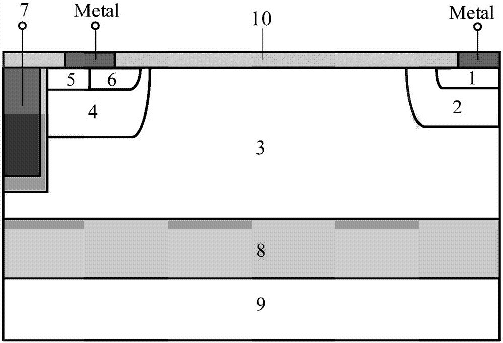
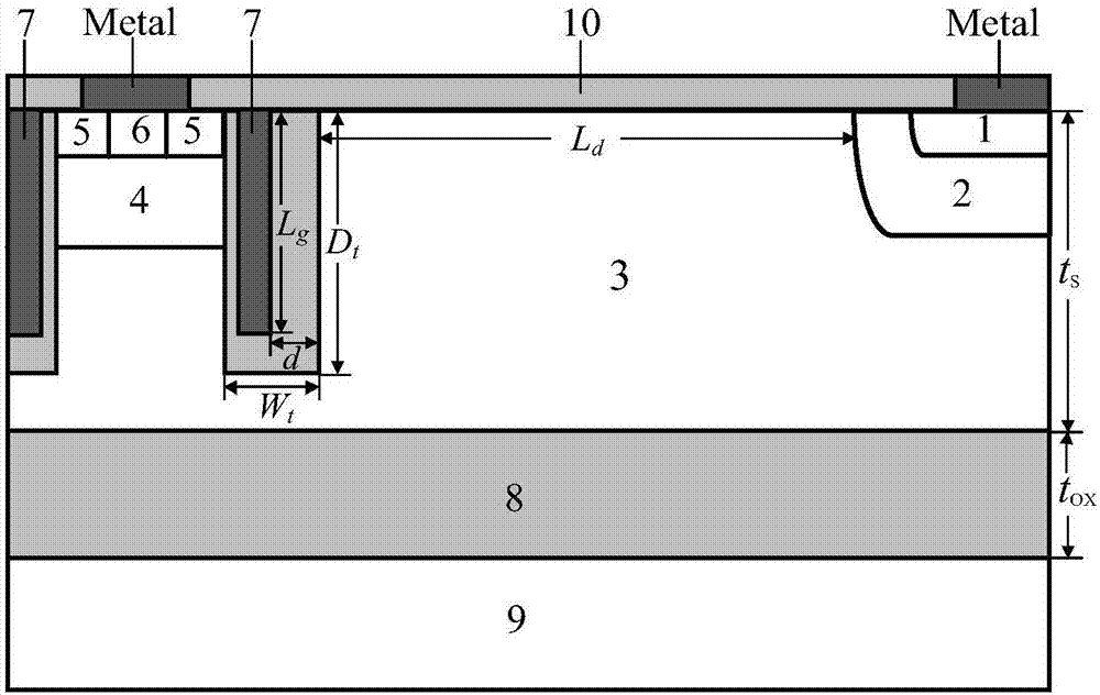
[0024] Such as figure 2 As shown, a low turn-off loss double-groove gate SOI-LIGBT device structure includes a P-type substrate 9, a buried oxide layer of silicon dioxide 8, an N-type drift region 3, and an N-type drift region 3 arranged in sequence from bottom to top. One end of the interior is provided with a P-type well region 4, the other end is provided with an N-buffer layer 2, and the surface of the device is provided with an oxide layer 10. The interior of the P-type well region 4 is provided with two N-type source terminals 5 and two N-buffer layers. The P-type contact region 6 between the source terminals 5; the N-type anode region 1 is provided above the inside of the N-buffer layer 2; the N-type source terminal 5, the P-type contact region 6 and the N-type anode region 1 are above A metal layer is provided; the left and right sides of the channel between the source end 5 and the P-type well region 4 are gate oxide layers, and polysilicon 7 is arranged next to the ...

Embodiment 2

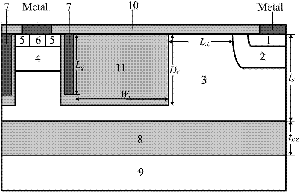
[0030] Such as image 3 As shown, the low turn-off loss double-groove gate SOI-LIGBT device structure of this embodiment is basically the same as that of Embodiment 1, the difference lies in: the inside of the N-type drift region 3 between the P-type well region 4 and the N-buffer layer 2 A silicon dioxide tank dielectric 11 is provided; the silicon dioxide tank dielectric 11 is located on the right side of the polysilicon 7 on the right side of the P-type well region 4 .

[0031] The minimum value of the width Wt of the silicon dioxide groove medium 11 is 1 μm.

[0032] Preferably, the right side of the silicon dioxide trough medium 11 may be in contact with the left side of the N-buffer layer 2 , that is, Ld is zero.

[0033] The depth of the silicon dioxide groove medium 11 is Dt, which is greater than the depth Lg of the polysilicon 7, and satisfies the thickness of the silicon layer, that is, the thickness t of the N-type drift region 3 s >D t ≥ L g +1um.

[0034] Sp...

Embodiment 3

[0039] Such as Figure 7 As shown, the low turn-off loss double-groove gate SOI-LIGBT device structure of this embodiment is basically the same as that of Embodiment 2, the difference is that an N-type carrier storage layer 12 is provided under the P-type well region 4 . Depth L of two polysilicon 7 g equal to and greater than the depth D of the N-type carrier storage layer 12 cs .

[0040] Specifically, the thickness t of the buried oxide silicon dioxide 8 ox is 3 μm, the thickness of the silicon layer is also the thickness t of the N-type drift region 3 s 4μm, the length L of the N-type drift region 3 d 13μm, doping concentration N d 2.5e15cm -3 , the gate oxide thickness is 20nm, the doping concentration N of the P-type well region 4 pwell 4e17cm -3 , the doping concentration of the N-type carrier storage layer 12 is 1e18cm -3 , the doping concentration of N-buffer layer 2 is 4e17cm -3 , polysilicon depth L g is 2.2 μm, the depth D of the silica groove dielectric...


PUM


Abstract

The invention provides a silicon on insulator-lateral insulated gate bipolar transistor (SOI-LIGBT) device structure with low switch-off loss and dual groove gates. The SOI-LIGBT device structure comprises a P-type substrate, buried oxide layer SiO2, an N-type drift region, a P-type well region, an N-buffer layer, an oxide layer, two N-type source ends, a P-type contact region and an N-type positive electrode region, wherein the P-type contact region is arranged between the two N-type source ends, gate oxide layers are arranged at two sides of a channel between the source ends and the P-type well region, and poly-silicon is arranged aside the gate oxide layers and is arranged at two sides of the P-type well region and at a left side of the N-buffer layer. The SOI-LIGBT device structure possesses a dual-gate structure and has higher current capability under the same condition, holes directly injected to the P-type well region are reduced by the introduction of an N-type carrier storage layer, so that the carrier distribution is more uniform, the carrier combination during switch off is facilitated, and the switch-off time is reduced; the effective space of the N-type drift region is reduced by groove medium SiO2, the injection of carriers at a right side is also simultaneously blocked, and a carrier accumulation layer is formed; and based on two effects, the switch-off loss of the structure is substantially reduced.

Description

technical field [0001] The invention belongs to the technical field of semiconductors, and in particular relates to a low turn-off loss double-groove gate SOI-LIGBT device structure. Background technique [0002] High-voltage power devices are the foundation and core of power electronics technology, which have the characteristics of high voltage resistance and high conduction current density. Improving the withstand voltage capability of power devices and reducing the turn-off loss of power devices is the key to designing devices. As an important class of power semiconductor devices, IGBT devices (insulated gate bipolar transistor devices) are widely used in the field of power electronics. However, due to the low hole injection efficiency and low carrier concentration distribution of the IGBT device at the junction of the P-body region and the N-drift region, the saturation voltage drop of the device increases. When it is turned off, the N-drift region A large number of mi...

Claims


Application Information

Patent Timeline
Patent Type & Authority Applications(China)
IPC IPC(8): H01L29/739H01L29/40H01L29/423
CPCH01L29/7393H01L29/40H01L29/4232
Inventor 乔明李路丁柏浪何逸涛杨文张波
Owner UNIV OF ELECTRONICS SCI & TECH OF CHINA
Why Eureka
Try Eureka