Image sensor chip packaging structure and packaging method

An image sensor and packaging method technology, which is applied to semiconductor devices, electric solid state devices, radiation control devices, etc., can solve the problems of complex packaging structure, difficult packaging process of wafer-level image sensors, and complex through-silicon via interconnection process, etc. To achieve the effect of simplifying the packaging structure and process, avoiding poor connection reliability and avoiding poor reliability

Active Publication Date: 2017-06-27
SEMICON MFG INT (SHANGHAI) CORP +1
View PDF5 Cites 8 Cited by
  • Summary
  • Abstract
  • Description
  • Claims
  • Application Information

AI Technical Summary

Problems solved by technology

However, due to the introduction of TSV interconnection in this wafer-level image sensor packaging method, the packaging structure is complicated; and TSV interconnection technology is still immature, often due to poor insulation in the hole, incomplete interconnection windows, and incomplete metal filling. Such problems lead to failure or poor reliability, which makes this kind of wafer-level image sensor packaging using through-silicon via interconnection have problems of high process difficulty and low interconnection reliability.
At the same time, the complexity of the through-silicon via interconnection process also makes the packaging price of the wafer-level image sensor using this technology relatively expensive.

Method used


Image

  • Image sensor chip packaging structure and packaging method
  • Image sensor chip packaging structure and packaging method
  • Image sensor chip packaging structure and packaging method

Examples


Embodiment Construction
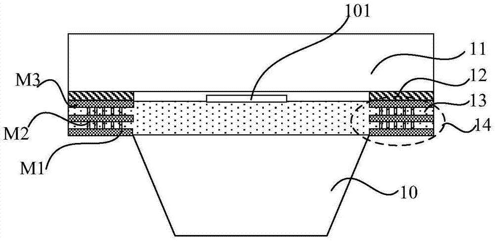
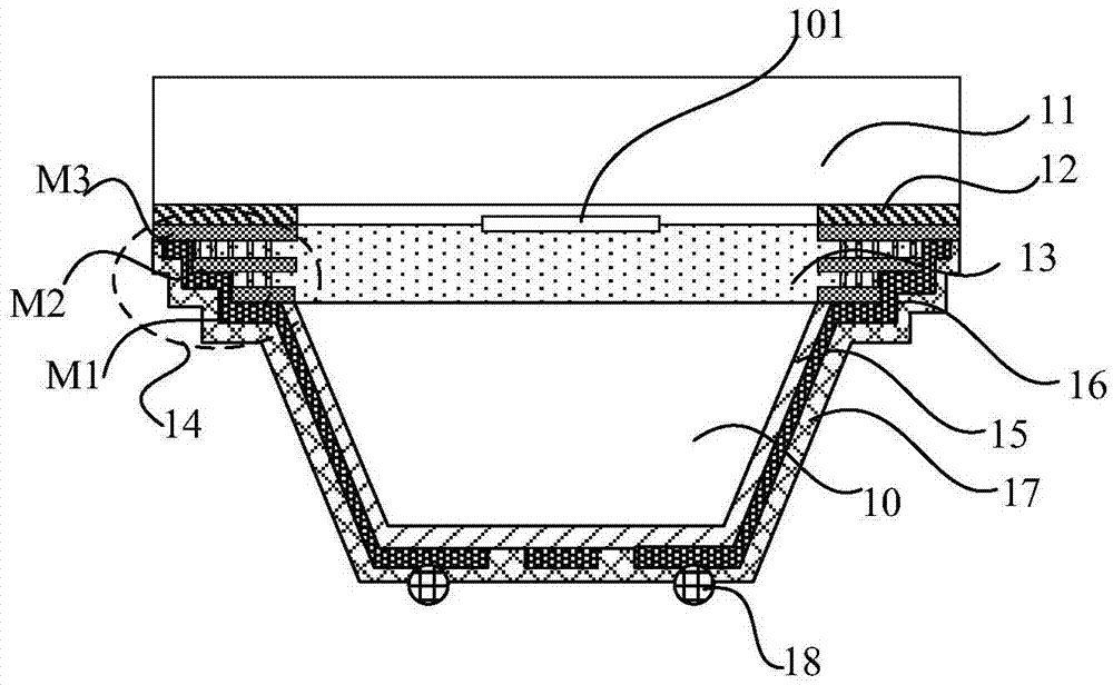
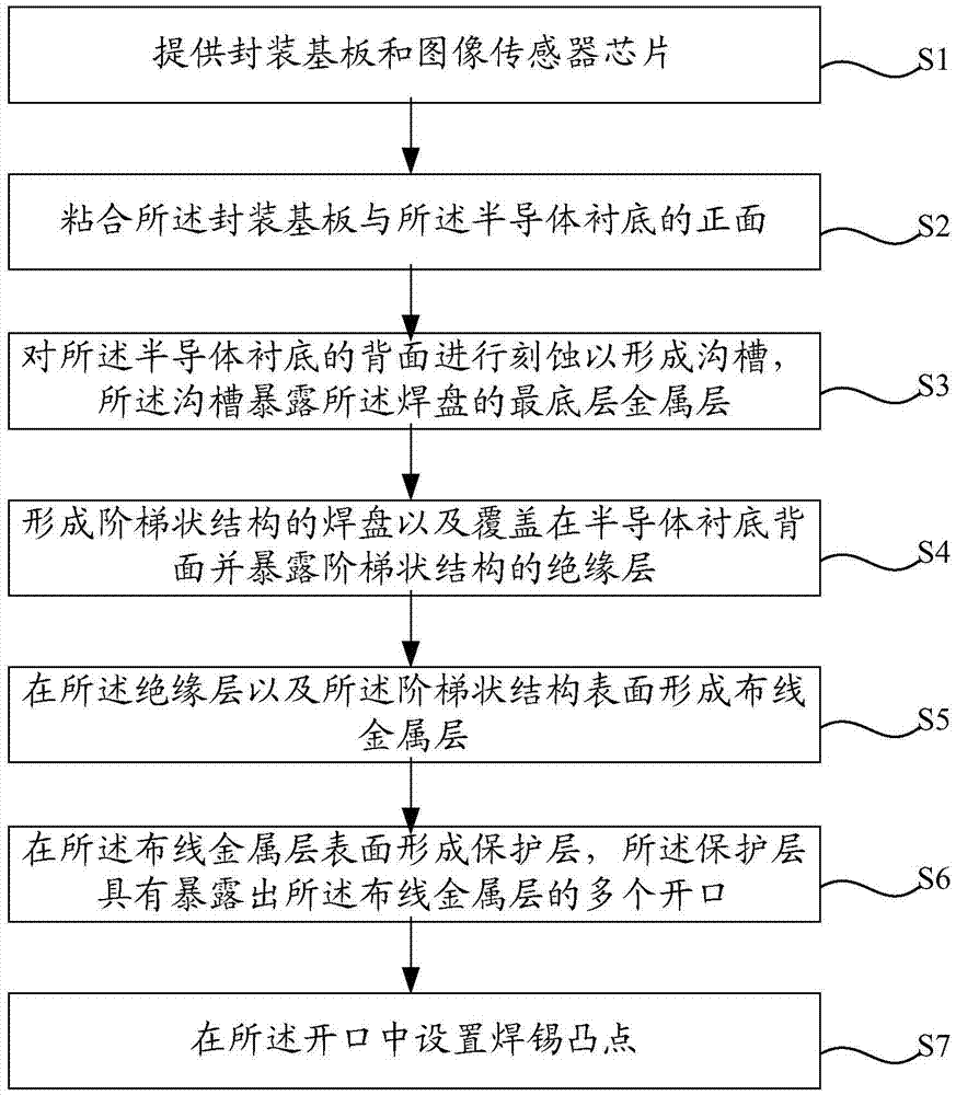
[0047] The core idea of ​​the present invention is to provide a non-through-silicon via, low-cost image sensor flip packaging process, which uses the substrate trench etching process on the back of the chip to avoid the use of the through-silicon via (TSV) process, and at the same time exposes the bottom of the trench The outer peripheral edge of the pad is modified into a stepped structure, thereby reducing the difficulty of filling the wiring metal layer, increasing the contact area between the subsequent filled wiring metal layer and the pad, and improving the connection reliability of the wiring metal layer.

[0048]In order to make the purpose and features of the present invention more obvious and understandable, the specific implementation of the present invention will be further described below in conjunction with the accompanying drawings. However, the present invention can be implemented in different forms and should not be limited to the described embodiments.

[0049...


PUM


Abstract

The invention provides an image sensor chip packaging structure and a packaging method. A chip back surface substrate groove etching process is adopted to avoid using a silicon piercing technology, the peripheral edge of a pad exposed at the bottom part of the groove is corrected to have a ladder-like structure, and thus, the filling difficulty of a wiring metal layer is reduced, the contact area between the subsequently-filled wiring metal layer and the pad is increased, and the wiring metal layer connection reliability is improved.

Description

technical field [0001] The invention relates to the technical field of semiconductor manufacturing, in particular to a packaging structure and a packaging method of an image sensor chip. Background technique [0002] The CMOS image sensor (CMOS Image Sensor, CIS) is an important part of the digital camera. The principle of its imaging is to sense light through the photosensitive device, so as to convert the light signal into an electrical signal, and then output the image. [0003] Currently, mainstream CIS chip packaging technologies include: CSP (Chip Scale Package), COB (Chip On Board) and FC (Flip Chip). Among them, CSP refers to the chip packaging technology in which the chip size package and the core size of the chip are basically the same. It is currently widely used in Wafer level (wafer level) packaging of low-end, low-pixel (2M pixels or below) image sensors. CSP packaging technology generally uses the front of the image sensor chip as a photosensitive window, use...

Claims


Application Information

Patent Timeline
Patent Type & Authority Applications(China)
IPC IPC(8): H01L27/146
CPCH01L27/14601H01L27/14636H01L27/14683
Inventor 何明
Owner SEMICON MFG INT (SHANGHAI) CORP
Why Eureka
Try Eureka