Multi-ring-based optical network-on-chip topology structure design method

An optical-on-chip network and topology technology, applied in the field of communication, can solve problems such as complex network structure, low scalability, and network congestion

Active Publication Date: 2017-06-30
XIDIAN UNIV
View PDF2 Cites 4 Cited by
  • Summary
  • Abstract
  • Description
  • Claims
  • Application Information

AI Technical Summary

Problems solved by technology

[0006] The purpose of the present invention is to overcome the deficiencies of the above-mentioned prior art, and propose a multi-ring-based optical on-chip network topology design method, which is used to solve the serious network congestion and low scalability existing in the existing optical on-chip network topology. and problems with complex network structures

Method used


Image

  • Multi-ring-based optical network-on-chip topology structure design method
  • Multi-ring-based optical network-on-chip topology structure design method
  • Multi-ring-based optical network-on-chip topology structure design method

Examples


Embodiment Construction

[0031] The present invention will be described in further detail below in conjunction with the accompanying drawings.

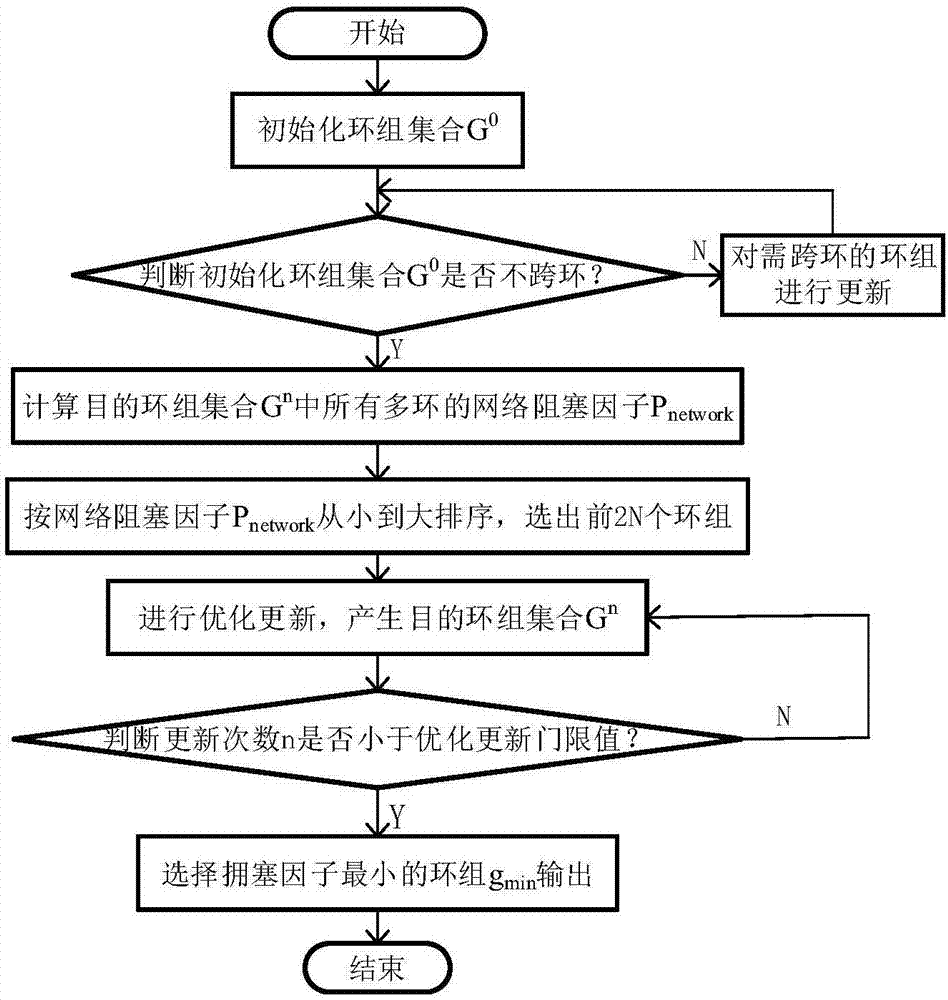
[0032] refer to figure 1 . A method for designing network topology on a multi-ring optical chip, comprising the steps of:

[0033] Step (1) Set ring group set G: including u ring groups g 1 , g 2 , g 3 ,...,g q ,...,g u , q represents the serial number of the ring group, and each ring group contains M rings R 1 , R 2 ,...,R r ,...,R M The multi-ring network topology, r represents the serial number of the ring, the multi-ring network topology contains N interconnected nodes, the ring group g q Each ring R in r Using a binary sequence C containing N bits 1×N , then the M rings can be represented by a two-dimensional array C M×N said, C M×N The bits in the rth row and the sth column are c r,s where 1≤r≤M, 1≤s≤N, and the rth ring does not contain the sth node in the topological network, use c r,s = 0 means that the r-th ring contains the s-th node ...


PUM


Abstract

The invention discloses a multi-ring-based optical network-on-chip topology structure design method, and is used for solving the problems of severe network congestion, low extensibility and complex network of the existing optical network-on-chip topology structure. The implementation steps are that a ring set collection G is set; the ring set collection G is initialized; whether each ring set gq in the initialized ring set collection G0 has no ring crossing is judged; the network congestion factors of all the ring sets in a target ring set collection Gn are calculated; the previous 2N ring sets of all the ring sets are selected according to ordering of the network congestion factors; the previous 2N ring sets are optimized and updated so that the target ring set collection Gn is obtained; and the updating number n is judged, and the ring set gmin of the lowest congestion probability factor is selected. The method of selecting the multi-ring topology of the lowest network congestion probability factor and the single wavelength communication method are adopted so that the congestion situation of the optical network-on-chip can be alleviated, the extensibility of the optical network-on-chip can be enhanced and the network complexity and cost can be reduced.

Description

technical field [0001] The invention belongs to the technical field of communication, and relates to a design method of an optical on-chip network topology structure, in particular to a design method of a multi-ring-based optical on-chip network topology structure, which can be used for optical interconnection between IP cores on a chip, and realizes the optical interconnection based on Low-blocking data transmission between IP cores in the optical circuit-switched optical network on chip improves the efficiency of inter-core communication. Background technique [0002] The optical network on chip, which optically interconnects numerous IP cores on the chip, has the advantages of high bandwidth, low power consumption, low delay and low electromagnetic interference, and can effectively solve a series of bottleneck problems in the network on chip. Therefore, optical network-on-chip has become a multi-core interconnection technology that has attracted much attention. At presen...

Claims


Application Information

Patent Timeline
Patent Type & Authority Applications(China)
IPC IPC(8): H04L12/24H04L12/801H04L12/933H04J14/02
CPCH04J14/0227H04J14/0283H04L41/14H04L47/127H04L49/109
Inventor 朱李晶顾华玺王琨杨银堂朱樟明刘良凯
Owner XIDIAN UNIV
Why Eureka
Try Eureka