

3D NAND memory device and manufacturing method therefor
A technology for storage devices and storage areas, which is applied in the field of flash memory, can solve the problems of increased numbers and the inability to integrate 3D NAND devices together, and achieve the effect of easy process integration
- Summary
- Abstract
- Description
- Claims
- Application Information
AI Technical Summary
Problems solved by technology
Method used
Image

Examples
Embodiment 1
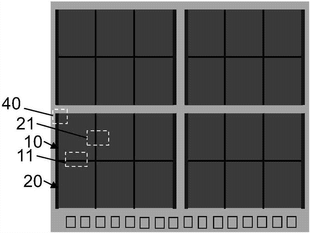
[0060] refer to figure 1 Shown is a schematic top view of a 3D NAND memory device chip according to an embodiment of the present invention. In this specific embodiment, the memory chip includes 4 plate storage areas, and in each plate (plate) storage area Contains multiple block storage areas. It can be understood that this is only an example, and there may be other design arrangements according to different designs, and the present invention is not limited thereto.
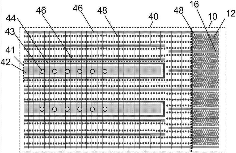
[0061] refer to figure 2 shown, for figure 1 A partially enlarged view of the middle region 40, which shows a ladder structure and a part of the first storage area. In the first storage area 10, a block is divided into three parts by grid line gaps, and each pair of grid line gaps There is a finger storage area in between, and the first storage area is an array area of 3D NAND storage units, which may contain one or more block storage areas.
[0062] In this embodiment, the grid line slits 46 of the ladder...
Embodiment 2
[0065] In this embodiment, parts different from those in Embodiment 1 will be described, and the same parts will not be repeated.
[0066] refer to image 3 shown, for figure 1 A partially enlarged view of the middle region 40, which shows a ladder structure and a part of the first storage area. In the first storage area 10, a block is divided into three parts by grid line gaps, and each pair of grid line gaps There is a finger storage area in between, and the first storage area is an array area of 3D NAND storage units, which may contain one or more block storage areas.
[0067] The sub-step region 41 is disposed between the gate line gaps of the corresponding block region of the step structure 40 , and the corresponding region of the step structure (not shown in the figure) on the other side is used for forming an interconnection structure. That is to say, the sub-step region 41 occupies the step structure region corresponding to a block region of the first storage regio...
Embodiment 3
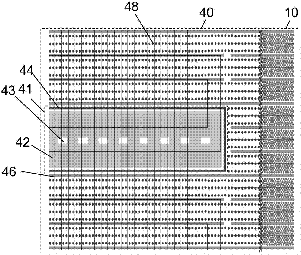
[0069] In addition, a through contact hole area can also be provided in the direction of the bit line for connection with the CMOS circuit chip, refer to figure 1 with Figure 4 as shown, Figure 4 for figure 1 A partially enlarged view of the middle area 11, a via hole formation area 20 is arranged between the first storage area 10 and the second storage area 30, and the first storage area 10, the via hole formation area 20 and the second storage area 30 are along the bit line Arranged in order, the same as the first storage area 10, the second storage area, 20 includes the word line stack layer and the channel hole 12 in the word line stack layer; the via hole formation area 20 includes a via stack of oxide layer and nitride layer layer 24 , the through contact hole 26 penetrating through the via stack layer 24 and the insulating layer 22 on the sidewall of the via stack layer; the gate line gap 16 along the word line direction in the first storage area 10 and the second s...
PUM
 Abstract
Description
Claims
Application Information