Display panel and display panel manufacturing method

A display panel and manufacturing method technology, applied in semiconductor/solid-state device manufacturing, semiconductor devices, electrical components, etc., can solve problems such as reduced adhesion, peeling, film peeling, etc., and achieve increased mechanical occlusal force and increased contact. Area, good contact effect

Active Publication Date: 2017-07-07
SHANGHAI TIANMA MICRO ELECTRONICS CO LTD
View PDF4 Cites 11 Cited by
  • Summary
  • Abstract
  • Description
  • Claims
  • Application Information

AI Technical Summary

Problems solved by technology

In order to improve the barrier performance of the inorganic layer, the inorganic layer is generally made denser and smoother, and when the organic layer is in contact with the dense and smooth inorganic layer, the adhesion between the two decreases, and the The organic layer is easy to loosen or even fall off, and the film layer on the inorganic layer will fall off, causing the display panel to fail to display normally

Method used


Image

  • Display panel and display panel manufacturing method
  • Display panel and display panel manufacturing method
  • Display panel and display panel manufacturing method

Examples


Embodiment Construction

[0024] The present invention will be further described in detail below in conjunction with the accompanying drawings and embodiments. It should be understood that the specific embodiments described here are only used to explain the present invention, but not to limit the present invention. In addition, it should be noted that, for the convenience of description, only some structures related to the present invention are shown in the drawings but not all structures.

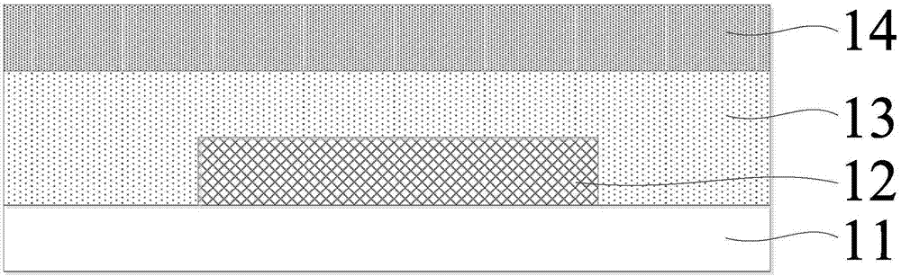
[0025] Figure 1A is a schematic cross-sectional structure diagram of a display panel provided by an embodiment of the present invention, see Figure 1A , the display panel includes:

[0026] Array substrate 11;

[0027] A plurality of organic light emitting elements 12 are located on one side of the array substrate 11;

[0028] The thin film encapsulation layer, the thin film encapsulation layer is located on the side of the plurality of organic light emitting elements 12 facing away from the array substrate 11 ...


PUM


Abstract

The embodiment of the invention discloses a display panel and a display panel manufacturing method. The display panel comprises an array substrate, a plurality of organic light-emitting elements arranged on one side of an array substrate, and a thin-film packaging layer located on one side of the organic light-emitting elements that is far away from the array substrate and used for covering the plurality of organic light-emitting elements. The thin-film packaging layer comprises at least one barrier layer. The surface roughness of the barrier layer is 0 nm-5 nm. One side of the at least one barrier layer, away from the array substrate, is provided with a roughness layer. The roughness layer is in contact with the barrier layer. The surface roughness of the roughness layer is larger than 5 nm. According to the technical scheme of the invention, on the basis that the reliable encapsulation of the display panel is effectively guaranteed, a film layer above the barrier layer can be firmly combined with the barrier layer. The peeling problem of the film layer is solved. The performance of the display panel is improved.

Description

technical field [0001] Embodiments of the present invention relate to the field of display technology, and in particular, to a display panel and a method for manufacturing the display panel. Background technique [0002] Compared with liquid crystal display panels, OLED (Organic Light Emitting Diode) display panels have the advantages of wide viewing angle, high contrast ratio, thinness, and low power consumption, and are currently one of the development directions of flat panel display technology. [0003] The OLED display panel in the prior art generally includes a substrate, an organic light emitting element on one side of the substrate, a thin film encapsulation layer and some other film layers on the thin film encapsulation layer. The thin film encapsulation layer generally includes stacked inorganic layers and organic layers, mainly relying on the inorganic layer to block moisture and oxygen from entering the organic light-emitting element. In order to improve the bar...

Claims


Application Information

Patent Timeline
Patent Type & Authority Applications(China)
IPC IPC(8): H01L27/32H01L51/52H01L51/56
CPCH10K59/12H10K50/844H10K71/00
Inventor 蔡雨李喜烈刘聪慧于泉鹏
Owner SHANGHAI TIANMA MICRO ELECTRONICS CO LTD
Why Eureka
Try Eureka