Infrared absorber based on dielectric microcolumn array and preparation method thereof

A technology of micro-column array and absorber, which is applied in the field of infrared absorber, can solve the problems of low quality factor of absorber and unstable absorption peak wavelength, etc., and achieve the effect of high absorption, high quality factor and high stability

Inactive Publication Date: 2017-07-14
HUAZHONG UNIV OF SCI & TECH +1
View PDF6 Cites 11 Cited by
  • Summary
  • Abstract
  • Description
  • Claims
  • Application Information

AI Technical Summary

Problems solved by technology

[0006] In view of the above defects, the purpose of the present invention is to provide an infrared absorber based on a dielectric micropillar array, which aims to solve the technical problems of low quality factor of the existing absorber and unstable absorption peak wavelength when the incident angle changes

Method used


Image

  • Infrared absorber based on dielectric microcolumn array and preparation method thereof
  • Infrared absorber based on dielectric microcolumn array and preparation method thereof
  • Infrared absorber based on dielectric microcolumn array and preparation method thereof

Examples


no. 1 example

[0048] The first embodiment of the method for preparing an infrared absorber based on a dielectric micropillar array provided by the present invention includes the following steps:

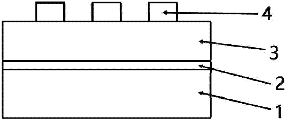
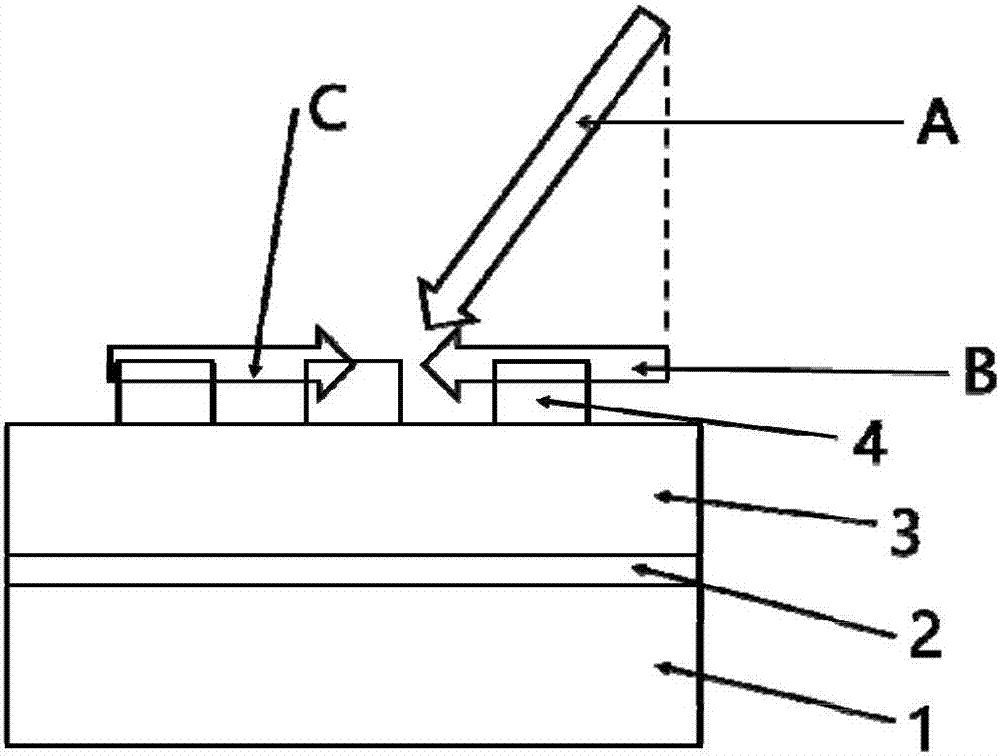
[0049] S1 Select a single crystal silicon with a thickness of 1000 μm as the substrate, first use acetone solution to ultrasonically clean the single crystal silicon for 3 minutes; then use an anhydrous ethanol solution to ultrasonically clean the single crystal silicon for 3 minutes; The crystalline silicon is ultrasonically cleaned for 2 minutes, and the gold powder is vaporized and condensed by electron beam evaporation equipment, thereby forming a 200nm gold-plated layer on the surface of the substrate and obtaining the first intermediate product.

[0050] S2 growing a silicon dioxide layer with a thickness of 1030 nm on the surface of the gold-plated layer of the first intermediate product by using a magnetron sputtering device to obtain a second intermediate product.

[0051] S3 On the silic...

no. 2 example

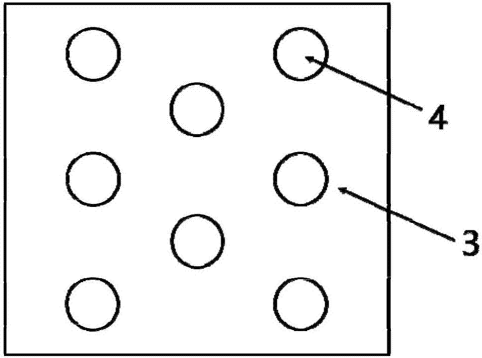
[0055] Second embodiment: Step S2 The thickness of the silicon dioxide layer is 1290 nm. In step S3, the diameter of the pillars in the dielectric micropillar array is 1100 nm, the height of the pillars is 680 nm, and the distance between the centers of two adjacent pillars is 2000 nm. The silicon grown in step S4 with a thickness of 680 nm.

[0056] Figure 5 For the infrared absorption spectrum of the infrared absorber finally obtained in the second embodiment provided by the present invention, when the laser incident angle is 0°, the wavelength of the absorption peak of the infrared absorption spectrum is located at 3.27 microns, and the absorption bandwidth is about 10.9 Nanometer, the figure of merit is about 300.

no. 3 example

[0057] Embodiment 3: Step S2 The thickness of the silicon dioxide layer is 1690 nm. In step S3, the diameter of the pillars in the dielectric micropillar array is 1430 nm, the height of the pillars is 890 nm, and the distance between the centers of two adjacent pillars is 2640 nm. The silicon grown in step S4 has a thickness of 890 nm.

[0058] Figure 6 For the infrared light absorption spectrum of the infrared absorber finally obtained in the third embodiment provided by the present invention, when the laser incident angle is 0°, the wavelength of the absorption peak of the infrared absorber is located at 4.26 microns, and the absorption bandwidth is about 21.3 Nanometer, quality factor is about 200.


PUM


Abstract

The invention discloses an infrared absorber based on a dielectric microcolumn array and a preparation method thereof. The infrared absorber includes a dielectric microcolumn array, a dielectric layer, and a metal layer, the dielectric microcolumn array is used to screen the wavelength of the incident light, the dielectric layer is used to enable the screened incident light to generate the electromagnetic wave, and the metal layer is used to convert the electromagnetic wave into the thermal energy for absorption. The infrared absorber has the advantages of high quality factor and narrow absorption peak width. When the column height is 630nm-1210nm, the column diameter is 809nm-1980nm, the center distance of the two adjacent columns is 1300nm-3600nm, and the thickness of the dielectric layer is 1030nm-2310nm, the Poynting vector of the dielectric microcolumn array surface is zero, and the absorption peak wavelength is independent of the incident angle within a certain range, the absorber quality factor can be higher than 100, and a narrow absorption peak bandwidth can be realized.

Description

technical field [0001] The invention belongs to the field of infrared absorbers, and more specifically relates to an infrared absorber based on a dielectric microcolumn array and a preparation method thereof. Background technique [0002] High performance infrared absorber is the key material of infrared detector. Researchers have long sought to improve the performance of infrared detectors through better infrared absorbers. In recent years, metasurfaces have come into people's field of vision as a brand-new electromagnetic material, and have been rapidly applied to the design and manufacture of infrared absorbers. [0003] The characteristic of a metasurface is that its electromagnetic properties are basically independent of the properties of its component materials, but related to its internal microstructure. When the incident light interacts with this layer of microstructure, surface plasmons are generated, which can realize the focusing and enhancement of the light fie...

Claims


Application Information

Patent Timeline
Patent Type & Authority Applications(China)
IPC IPC(8): G02B5/20G02B5/22
CPCG02B5/208G02B5/22
Inventor 易飞常晟源李君宇谈小超杨奥郭颂蒋顺周仑
Owner HUAZHONG UNIV OF SCI & TECH
Why Eureka
Try Eureka