Array substrate, display apparatus and manufacturing method therefor

A technology of array substrates and substrate substrates, which is applied in semiconductor/solid-state device manufacturing, electrical components, electric solid-state devices, etc., can solve problems such as reduced reliability, leakage, and inability to repair polysilicon, so as to improve reliability and reduce leakage problems Effect

Active Publication Date: 2017-08-08
TCL CHINA STAR OPTOELECTRONICS TECH CO LTD
View PDF5 Cites 12 Cited by
  • Summary
  • Abstract
  • Description
  • Claims
  • Application Information

AI Technical Summary

Problems solved by technology

However, in the preparation process, if the ILD film layer is not properly selected, the polysilicon cannot be fully repaired during the hydrogenation process, which will eventually lead to leakage, or too many hydrogen atoms will penetrate into the oxide semiconductor layer, resulting in reduced reliability. The problem

Method used


Image

  • Array substrate, display apparatus and manufacturing method therefor
  • Array substrate, display apparatus and manufacturing method therefor
  • Array substrate, display apparatus and manufacturing method therefor

Examples


Embodiment Construction

[0019] The present invention will be described in detail below in conjunction with the accompanying drawings and embodiments.

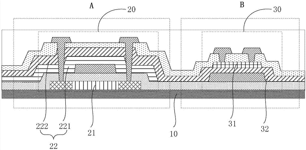
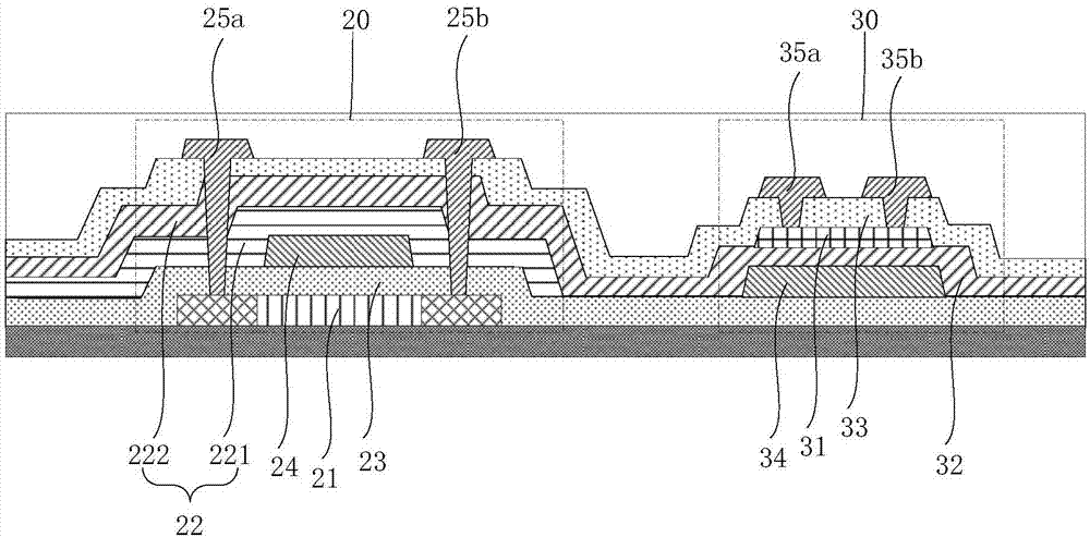
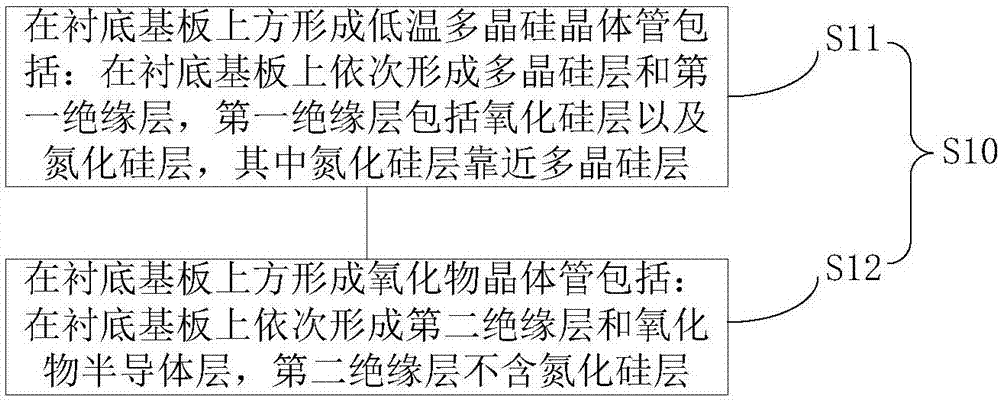
[0020] see figure 1 , figure 1 It is a schematic structural diagram of an embodiment of the array substrate of the present invention, the array substrate includes: a base substrate 10 and a low-temperature polysilicon transistor 20 and an oxide transistor 30 located above the base substrate 10, a display area B and a display area B are arranged on the substrate. In the non-display area A around the area B, the low temperature polysilicon transistor 20 is located in the non-display area A, and the oxide transistor 30 is located in the display area B. Wherein, the low-temperature polysilicon transistor 20 includes a polysilicon layer 21 and a first insulating layer 22 stacked, and the first insulating layer 22 includes a silicon oxide layer 222 and a silicon nitride layer 221, wherein the silicon nitride layer 221 is located between the polysilicon lay...


PUM


Abstract

The invention discloses an array substrate, a display apparatus and a manufacturing method therefor. The array substrate comprises a substrate, and a low-temperature poly-silicon transistor and an oxide transistor positioned above the substrate, wherein the low-temperature poly-silicon transistor comprises a poly-silicon layer and a first insulating layer which are arranged in a stacked manner; the first insulating layer comprises a silicon oxide layer and a silicon nitride layer, wherein the silicon nitride layer is positioned between the poly-silicon layer and the silicon oxide layer; the oxide transistor comprises an oxide semiconductor layer and a second insulating layer which are arranged in a stacked manner; and the second insulating layer does not comprise the silicon nitride layer. By virtue of the way, the electric leakage problem of the low-temperature poly-silicon transistor is effectively lowered, and meanwhile, the reliability of the oxide transistor is improved.

Description

technical field [0001] The present invention relates to the technical field of planar display, in particular to an array substrate, a display device and a manufacturing method thereof. Background technique [0002] Flat-panel display devices have many advantages such as thin body, power saving, and no radiation, and have been widely used. Existing flat panel display devices mainly include liquid crystal display devices (Liquid Crystal Display, LCD) and organic light emitting diode display devices (Organic Light Emitting Display, OLED), and active-matrix organic light emitting diodes (Active-matrix organic light emitting diode, AMOLED) has significant advantages over LCD in terms of energy consumption, color saturation, contrast, and flexible applications, and is widely used. [0003] The inventors of the present application have discovered during long-term research and development that since the active matrix organic light-emitting diode (AMOLED) panel is driven by current,...

Claims


Application Information

Patent Timeline
Patent Type & Authority Applications(China)
IPC IPC(8): H01L27/12H01L21/77
CPCH01L27/1225H01L27/1237H01L27/1259H01L27/1248H01L27/1251H01L27/1218H01L27/1262H01L27/127
Inventor 刘兆松徐源竣李松杉
Owner TCL CHINA STAR OPTOELECTRONICS TECH CO LTD
Why Eureka
Try Eureka