Method for measuring mobility of graphene microcell with semiconductor as substrate

A technology of graphene micro-domain and semiconductor, which is applied in the field of mobility measurement of graphene micro-domain, and can solve problems such as the influence of mobility

Active Publication Date: 2017-08-11
SUZHOU INST OF NANO TECH & NANO BIONICS CHINESE ACEDEMY OF SCI
View PDF7 Cites 7 Cited by
  • Summary
  • Abstract
  • Description
  • Claims
  • Application Information

AI Technical Summary

Problems solved by technology

However, in practical applications, the substrate of graphene is not limited to hBN. In most cases, graphene is not in a suspended state. Therefore, when graphene is integrated with semiconductors in micro-nano electronic and optoelectronic devices, graphite The influence of semiconductor mobility on ene mobility will be unavoidable

Method used


Image

  • Method for measuring mobility of graphene microcell with semiconductor as substrate

Examples


Embodiment Construction

[0014] The specific implementation of the method for measuring the mobility of graphene micro-domains with a semiconductor substrate as provided by the present invention will be described in detail below in conjunction with the accompanying drawings.

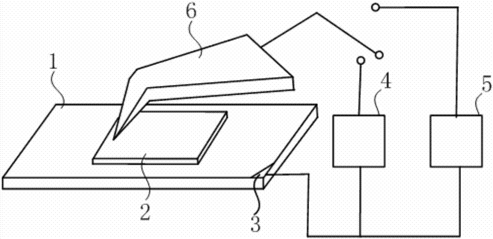
[0015] figure 1 It is a device diagram of the method for measuring the mobility of graphene micro-domains with semiconductor as substrate in the present invention. see figure 1 , the present invention's measurement takes semiconductor as the method for the graphene micro-region mobility of substrate comprising the steps:

[0016] Step S10, preparing samples.

[0017] Select the required semiconductor substrate 1, arrange ohmic contact electrodes 3 and cover graphene 2 on the surface of the semiconductor substrate 1, and connect the scanning Kelvin probe force microscope (KPFM) measurement module 4 and the conductive atomic force microscope (CAFM) measurement module 5 in parallel The two ends are respectively electrically conn...


PUM


Abstract

The invention provides a method for measuring the mobility of a graphene microcell with a semiconductor as a substrate. The method comprises steps of coating the surface of the semiconductor substrate with graphene to form a graphene microcell and disposing a conductive probe in contact with the graphene microcell; connecting the conductive probe with a scanning Kelvin probe force microscope to measure the actual work function of the graphene microcell to obtain a barrier height [Phi]Bn0 between the graphene microcell and the semiconductor substrate; connecting the conductive probe with a conductive atomic force microscope to collect a current-voltage curve of the graphene microcell; analyzing and fitting the current-voltage curve according to the barrier height [Phi]Bn0 between the graphene microcell and the semiconductor substrate and a hot electron emission model to obtain the effective contact radius of the conductive probe and the graphene microcell; and calculating the value of the graphene microcell mobility [mu] based on the effective contact radius of the conductive probe and the graphene microcell and the actual contact radius. The method can measure the mobility of the graphene microcell with any semiconductor as the substrate.

Description

technical field [0001] The invention relates to the field of graphene micro-domain mobility measurement, in particular to a method for measuring the mobility of graphene micro-domains with a semiconductor as a substrate. Background technique [0002] The magnitude of graphene mobility can directly evaluate the operating frequency and speed of graphene-based devices and circuits. The conventional measurement method of graphene mobility is to cover graphene on a silicon dioxide insulating substrate and use the Hall effect method for measurement. However, in the research on the device application of actual graphene and semiconductor construction, it is found that the mobility of graphene is easily affected by the substrate. In order to obtain the real mobility of graphene as accurately as possible, people usually spread graphene on the hBN substrate which has little influence on the mobility of graphene, because the lattice mismatch between hBN and graphene is only 1.8%. Alte...

Claims


Application Information

Patent Timeline
Patent Type & Authority Applications(China)
IPC IPC(8): G01R31/00
CPCG01R31/00
Inventor 钟海舰刘争晖徐耿钊徐科
Owner SUZHOU INST OF NANO TECH & NANO BIONICS CHINESE ACEDEMY OF SCI
Why Eureka
Try Eureka