Semiconductor structure and formation method thereof
A semiconductor and isolation structure technology, applied in the field of semiconductor structure and its formation, can solve the problem of difficult control of the fin height of transistors, achieve good electrical performance, reduce difficulty, and reduce the effect of impact
- Summary
- Abstract
- Description
- Claims
- Application Information
AI Technical Summary
Problems solved by technology
Method used
Image

Examples
Embodiment Construction
[0031] There are many problems in the formation method of the semiconductor structure in the prior art, for example, it is difficult to control the fin height of the fin field effect transistor.
[0032] Combining with the semiconductor structure of the prior art, the reasons why it is difficult to control the fin height of the semiconductor structure are analyzed:
[0033] Figure 1 to Figure 5 It is a structural schematic diagram of each step of a method for forming a semiconductor structure. The method for forming the semiconductor structure includes:
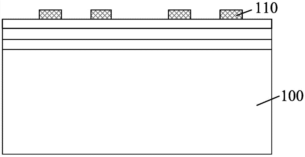
[0034] Please refer to figure 1 , providing a substrate 100 , and forming a mask layer 110 on the substrate 100 .
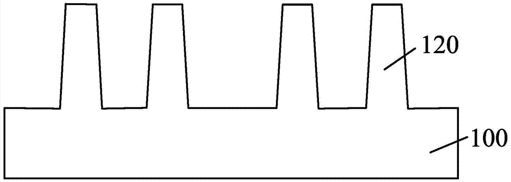
[0035] Please refer to figure 2 , using the mask layer 110 as a mask to etch the substrate 100 to form initial fins 120 .
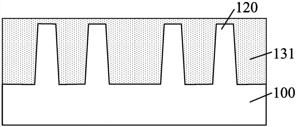
[0036] Please refer to image 3 , forming an isolation layer 131 covering the initial fin portion 120 .
[0037] Please refer to Figure 4 , the isolation layer 131 is planarized ...
PUM
| Property | Measurement | Unit |
|---|---|---|
| Thickness | aaaaa | aaaaa |
| Thickness | aaaaa | aaaaa |
| Thickness | aaaaa | aaaaa |
Abstract
Description
Claims
Application Information
 - Generate Ideas
- Intellectual Property
- Life Sciences
- Materials
- Tech Scout
- Unparalleled Data Quality
- Higher Quality Content
- 60% Fewer Hallucinations
Browse by: Latest US Patents, China's latest patents, Technical Efficacy Thesaurus, Application Domain, Technology Topic, Popular Technical Reports.
© 2025 PatSnap. All rights reserved.Legal|Privacy policy|Modern Slavery Act Transparency Statement|Sitemap|About US| Contact US: help@patsnap.com