

Mask plate including monitoring pattern and monitoring method
A mask plate and graphics technology, which is applied to the photoplate making process of the pattern surface, the original parts used for photomechanical processing, and instruments, can solve the problems of mask plate quality misjudgment and low yield rate of semiconductor products, and achieve Avoid the loss of product yield and improve the effect of reliability
- Summary
- Abstract
- Description
- Claims
- Application Information
AI Technical Summary
Problems solved by technology
Method used
Image

Examples
Embodiment Construction
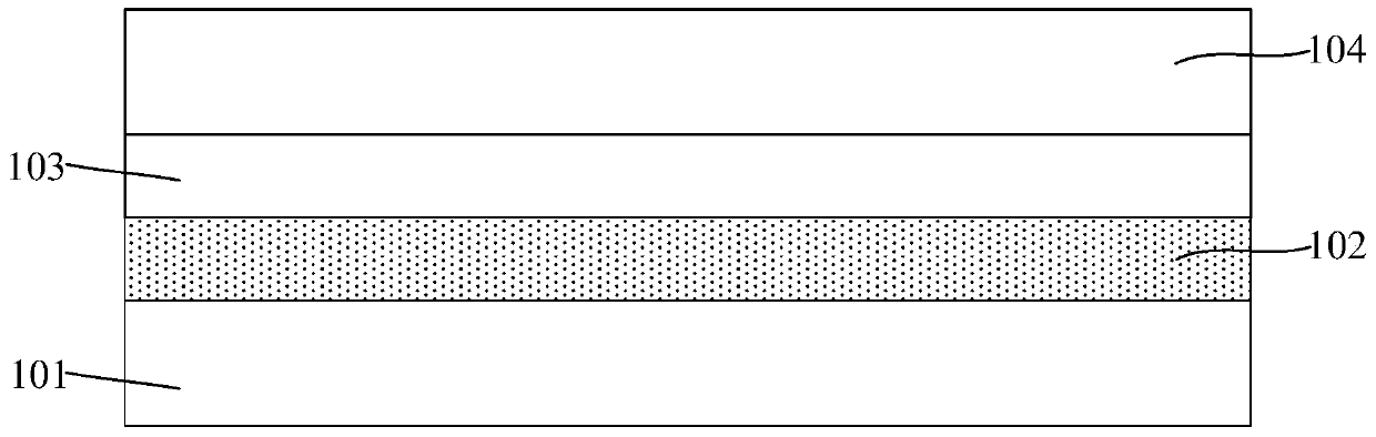
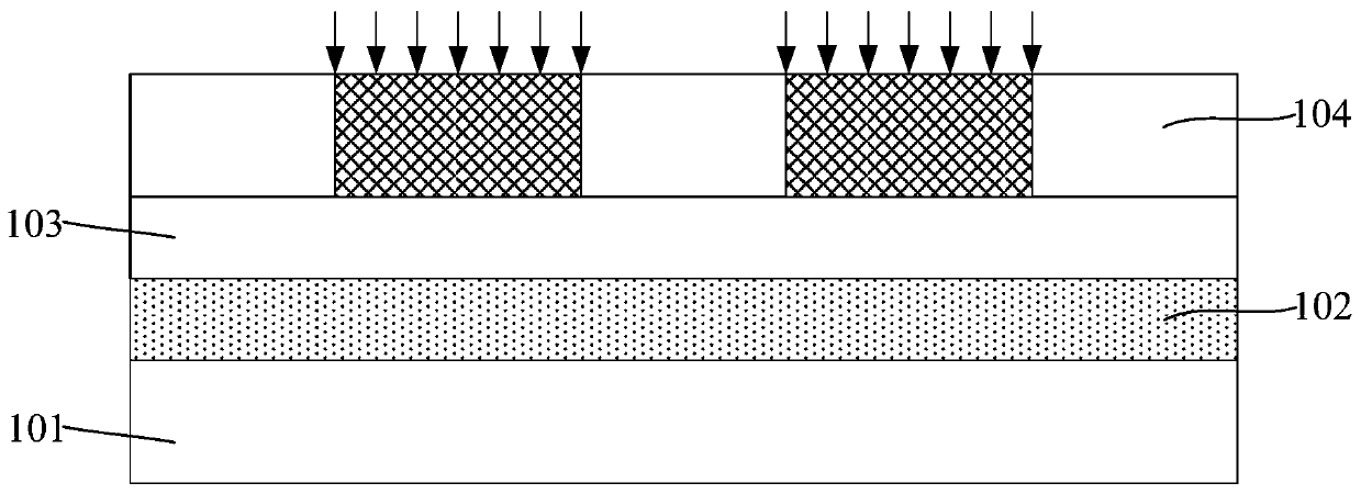
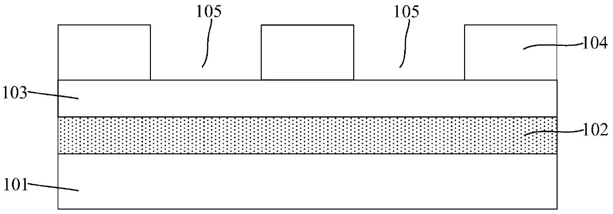
[0035] It can be known from the background art that in the prior art, after the geometrical figure defining the design pattern is formed on the mask plate, the subsequent process of semiconductor manufacturing is performed with the mask plate, which easily brings loss to the product yield.
[0036]After the design pattern is defined in the mask, the monitoring means of the mask is usually to monitor the top view of the mask (mask top view). Specifically, first obtain the top view of the mask with the design pattern defined SEM (Scan Electron Microscope) diagram of the view. When there is no problem with the information displayed in the top view, it is determined that the manufactured mask meets the requirements, and the design pattern in the mask is determined to be free of defects, so the manufactured mask can be put into the subsequent semiconductor process flow.
[0037] After analysis, it was found that in mask manufacturing, even if the information displayed in the above-...
PUM
 Abstract
Description
Claims
Application Information